Introduction
In industrial control, communication equipment, smart grids, and security systems, numerous signal interfaces need to connect to external lines, which are susceptible to lightning strikes, switching operations, electrostatic discharge (ESD), and electrical transient interference.
When abnormal overvoltages enter the equipment, communication chips, MCUs, and interface ICs may be damaged due to transient high voltage. Therefore, reliable overvoltage protection devices are required in communication interfaces such as RS485, CAN, RS422, and SLIC.
Common protection solutions include TVS diodes (Transient Voltage Suppressors), GDT gas discharge tubes, and TSS semiconductor discharge tubes.
Among them, the TSS (Thyristor Surge Suppressor) is a switching overvoltage protection device based on a PNPN structure, featuring low leakage current, fast response, low forward voltage, and low residual voltage, and is widely used in communication lines and industrial interface protection.
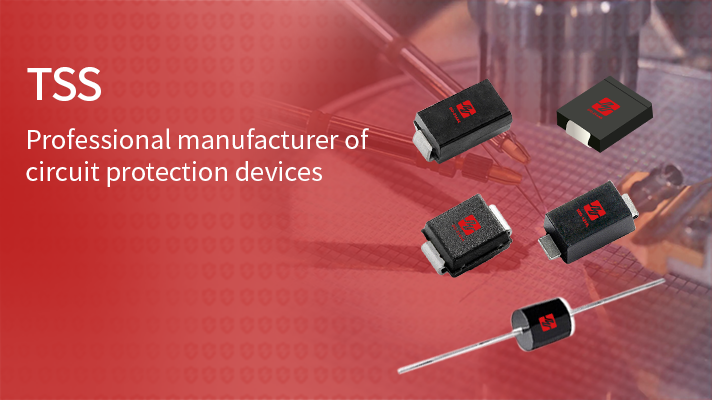
I. What is a TSS Semiconductor Discharge Tube?
A TSS (Thyristor Surge Suppressor) is a PNPN four-layer structure protection device manufactured using semiconductor technology. Its electrical characteristics are similar to a thyristor (SCR), exhibiting typical switching characteristics.
TSS Working Principle
- Normal Operation: The TSS is in a high-impedance cutoff state, having almost no impact on circuit operation.
- In the event of a surge or overvoltage: When an external abnormal voltage exceeds the TSS trigger voltage, the device quickly enters the conduction state, bypassing and discharging the surge current.
- After the surge subsides: When the current flowing through the TSS decreases below the holding current, the device automatically returns to the high-impedance cutoff state.
Unlike a TVS diode, the TSS does not absorb surge energy through clamping voltage, but rather forms a low-impedance path through rapid conduction, guiding the overvoltage to ground, thereby protecting downstream electronic equipment.
II. TSS Main Parameter Description
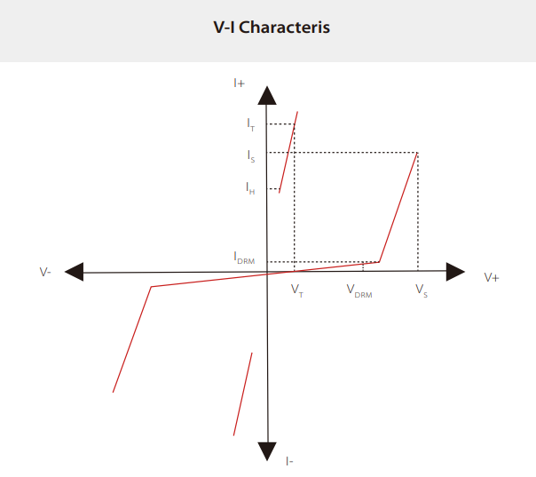
- Off-State Voltage VRM and Leakage Current IRM: The off-state voltage VRM represents the highest voltage at which the semiconductor overvoltage protector does not conduct. At this voltage, there is only a very small leakage current IRM.
- Breakdown Voltage VBR: The voltage at which a specified test current IR (typically 1mA) is applied. This is the voltage at which the semiconductor overvoltage protector begins to conduct.
- Breakpoint Voltage VBO and Breakpoint Current IBO: When the voltage rises to the breakpoint voltage VBO (corresponding to the breakpoint current IBO), the semiconductor overvoltage protector fully conducts, exhibiting very low impedance, and the voltage VT across it immediately drops to a very low value (typically around 5V).
- Peak Pulse Current IPP: The maximum pulse current that the semiconductor overvoltage protector can withstand.
- Holding Current IH: The minimum current required for the semiconductor overvoltage protector to remain in the conducting state. Once the current flowing through it falls below the holding current IH, it returns to the off state.
- Static Capacitance C: The capacitance value of the semiconductor overvoltage protector in its static state.
III. Main Characteristics of TSS
1) Low Leakage Current
In the untriggered state, the TSS exhibits high resistance, and the leakage current is typically only a few microamps or even lower.
2) Low On-Side Voltage
Upon triggering, the device quickly enters a low-impedance state, with an on-side voltage typically only a few volts. This effectively reduces surge residual voltage and protects downstream chips.
3) Fast Response
TSS response speeds typically reach the nanosecond level, enabling rapid response to lightning-induced surges, EFT (Electronic Fast Transmission), and ESD (Electrostatic Discharge).
4) Bidirectional Protection
Most TSSs exhibit bidirectional symmetrical characteristics, allowing simultaneous protection against both forward and reverse surges.
5) Good Trigger Voltage Consistency
Compared to traditional discrete protection solutions, TSSs offer more stable breakdown characteristics.
III. Limitations of TSS
1) Lower Surge Capacitance than GDT (Gas Thrust Damage)
GDTs can achieve kA-level surge capacity, while TSSs typically range from tens to hundreds of A.
Therefore, TSSs are primarily used for communication signal lines, rather than large power supply surge protection.
2) Relatively High Capacitance
TSS parasitic capacitance typically ranges from tens to hundreds of pF. For high-speed interfaces, low-capacitance models need to be selected.
3) Limited voltage level selection
TSS typically offers fixed voltage levels, requiring selection based on system voltage matching.
IV. TSS vs TVS vs GDT Comparison
| Feature | TSS | TVS | GDT |
| Protection Method | Switching protection | Voltage clamping | Gas discharge |
| Response Speed | ns level | ps-ns level | μs level |
| Residual Voltage | Very low | Medium | Lowest |
| Leakage Current | μA level | μA level | Extremely low |
| Surge Capability | Tens to hundreds of A | Tens to hundreds of A | kA level |
| Main Applications | Communication interfaces | Power and signal protection | Lightning surge protection |
In simple terms,
TSS: Suitable for communication interface protection, prioritizing low residual voltage.
TVS: Suitable for fast clamping protection.
GDT: Suitable for high-energy lightning surge discharge.
In practical designs, a combination of GDT and TSS is often used to achieve multi-level protection.
V. TSS Selection Guides
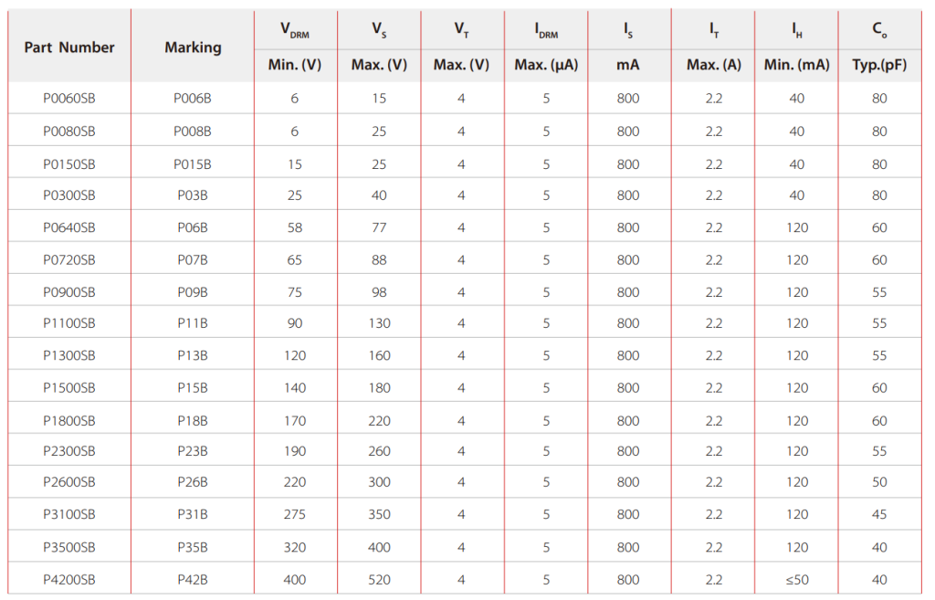
1) VDRM: The cutoff voltage must be greater than the maximum operating voltage of the protected circuit and less than the maximum limiting voltage. Otherwise, it will not only affect the normal operation of the protected circuit, but also the lifespan of the TSS;
2) VS: The breakover voltage must be greater than the normal operating voltage of the equipment signal, and less than the maximum limit voltage of the equipment;
3) IH: The holding current must be greater than the operating current of the equipment;
4) C: The parasitic capacitance is selected according to the allowable insertion loss of the circuit or the frequency of signal transmission;
5) IPP: The maximum instantaneous peak current IPP must be greater than the value specified in the communication equipment standard;
6) Pw: When the semiconductor discharge tube is in the conducting state, the power dissipated should be less than its rated power;
7) Because the semiconductor discharge tube is a switching overvoltage protection device, the voltage is relatively low after conduction, therefore it cannot be used alone in high power line protection;
8) It is generally connected in parallel in the circuit.
Conclusion
Semiware offers a variety of semiconductor protection devices, including:
- TSS Thyristor Surge Suppressor
- TVS Diodes
- ESD Protection Devices
- PLED Open LED Protectors
- GDT Gas Discharge Tubes
These products are widely used in:
- RS485/RS422 interfaces;
- CAN bus;
- Industrial communication equipment;
- Security systems;
- Smart meters;
- SLIC line protection.
If you are designing surge protection for communication interfaces, the Semiware technical team can provide suitable protection solutions based on operating voltage, communication speed, and surge level.