As the two primary types of MOSFETs (Metal-Oxide-Semiconductor Field-Effect Transistors), NMOS and PMOS share structural similarities but exhibit significant differences in terms of performance, power consumption, and application scenarios.
This article will provide an in-depth analysis of the differences between NMOS and PMOS, their structural principles, and how—through their "complementary" nature—they have become a classic combination in modern circuit design.
I. What is NMOS? The "King of Speed"
NMOS, or N-channel Metal-Oxide-Semiconductor, is characterized primarily by its use of electrons as the majority carriers for conduction.
Operating Principle:
When a positive voltage is applied to the gate relative to the source:
- Electrons are attracted to the region beneath the gate.
- A conductive channel forms between the source and the drain.
- Current begins to flow.
Advantages of NMOS:
- High electron mobility → Fast switching speeds.
- Smaller device size → Suitable for high-density circuit integration.
- Low on-resistance → Strong driving capability.
Disadvantages of NMOS:
- Power Consumption Challenges: In early logic circuits, NMOS devices often consumed more power when in the "on" state.
- Noise Margin: Compared to PMOS, NMOS exhibits slightly weaker noise immunity in certain specific circuit configurations.
II. What is PMOS? The "Robust Guardian"
PMOS, or P-channel Metal-Oxide-Semiconductor, utilizes holes as its majority carriers.
Operating Principle:
When a negative voltage is applied to the gate relative to the source:
- Holes accumulate in the gate region.
- A conductive channel forms.
- Current conduction is established.
Advantages of PMOS:
- Lower leakage current (under specific conditions).
- Stronger noise immunity.
- Frequently used for power-side control and in complementary structures.
Disadvantages of PMOS:
- Speed and Size: Constrained by the lower mobility of holes, PMOS devices exhibit slower switching speeds.
III. NMOS vs. PMOS: A Comparison of Core Differences
| Aspect | NMOS | PMOS |
| Majority Carriers | Electrons | Holes |
| Semiconductor Type | n-type | p-type |
| Gate Control | Turns ON when Gate is positive vs Source | Turns ON when Gate is negative vs Source |
| Operation Mode | Conducts with positive Vgs | Conducts with negative Vgs |
| Carrier Mobility | Higher (electron mobility) | Lower (hole mobility) |
| Switching Speed | Faster | Slower |
| On-Resistance (Rds(on)) | Lower (same size) | Higher (same size) |
| Efficiency | Higher efficiency | Lower efficiency |
| Typical Usage | Low-side switching, high-speed circuits | High-side switching, load control |
| CMOS Role | Pull-down network | Pull-up network |
| Applications | DC-DC converters, motor drivers, digital ICs | Load switches, battery protection, CMOS logic |
👉 NMOS is better suited for speed-oriented applications, while PMOS is better suited for stability and power-side applications.
IV. Application Scenarios: Specialized Roles and Powerful Partnerships
In modern electronic design, NMOS and PMOS rarely "operate alone"; instead, they most frequently appear in complementary configurations.
1. NMOS's Primary Domain:
Low-Side Driving: The source is connected to ground, while the load is connected between the drain and the power supply. Due to their low on-resistance and minimal heat generation, they are ideally suited for high-power switching applications such as motor control and LED driving.
High-Speed Digital Logic: The pull-down networks within CPUs are composed almost entirely of NMOS transistors, designed to achieve the ultimate in computational speed.
2. PMOS's Primary Domain:
High-Side Driving: The source terminal is connected to the positive power supply rail. PMOS transistors can function as power switches to control the on/off state of a load.
Analog Switching: Leveraging the compatibility of PMOS transistors with wide signal voltage swings, they are frequently employed in analog multiplexers.
👉 NMOS transistors handle pull-down operations, while PMOS transistors handle pull-up operations; working in a complementary fashion, they enable efficient, low-power logic control.
V. Structural Differences
Although NMOS and PMOS transistors appear similar in their circuit symbols, at the microscopic level, they are "mirror images" of one another.
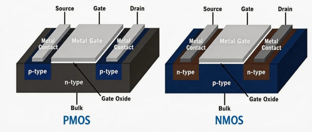
NMOS Structure:
- Substrate: P-type semiconductor
- Source/Drain: N-type diffusion regions
- Turn-on Condition: A positive voltage is applied to the gate.
PMOS Structure:
- Substrate: N-type semiconductor
- Source/Drain: P-type diffusion regions
- Turn-on Condition: A negative voltage is applied to the gate.
VI. Practical Selection Guidelines
✅ When should you choose NMOS?
- When high-speed switching is required
- For low-side switching applications
- For motor driving and power management systems
- For digital logic circuits
✅ When should you choose PMOS?
- For high-side switching applications
- For battery-powered systems
- When superior noise immunity is required
- For power path control
Summary
NMOS and PMOS transistors are the two fundamental building blocks of modern electronic systems. Each offers distinct advantages regarding carrier type, switching speed, power consumption characteristics, and application scenarios.
👉 Browse our MOSFET Product Series: https://en.semiware.com/product-line/mosfets/
In practical engineering design, the choice between NMOS and PMOS requires careful consideration of the specific application context to achieve the optimal combination and match.
If you are currently engaged in circuit design or component selection, we can provide you with expert support:
- Circuit protection and component selection recommendations (NMOS, PMOS, ESD protection, TVS diodes, etc.)
- Optimized solutions tailored to specific applications (power supplies, motor drives, IoT devices, etc.)
- Critical parameter matching and recommendations for alternative components
- Comprehensive solutions for EMC/ESD protection
👉 Please feel free to contact us for complimentary technical support or to request samples for testing.


Comments (0)