Overview
MOSFET (Metal Oxide Semiconductor Field Effect Transistor) is a semiconductor device widely used for switching purposes and amplification of electronic signals in electronic devices. Due to its very small size, MOSFET can be both a core and an integrated circuit and can be designed and manufactured in a single chip. The introduction of MOSFET devices brought changes in the field of electronic switching.
What is the mosfet?
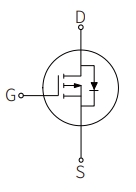
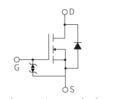
The MOSFET is a four-terminal device with source, gate, drain, and body terminals. Typically, the body of a MOSFET is connected to the source terminal, forming a three-terminal device such as a field effect transistor. MOSFETs are often considered transistors and are used in both analog and digital circuits.
According to the above MOSFET structure, the functioning of MOSFET depends on the electrical changes that occur in the channel width and the flow of carriers (holes or electrons). The charge carriers enter the channel through the source terminal and leave through the drain.
The width of the channel is controlled by the voltage on an electrode called the gate, which is located between the source and drain. It is insulated from the channel by a very thin metal oxide layer nearby. The MOS capacity present in the device is a critical part of the entire operation.
Working Principle of Mosfet
The main principle of the MOSFET device is the ability to control the voltage and current between the source terminal and the drain terminal. It works almost like a switch and the functioning of the device is based on the MOS capacitor. The MOS capacitor is the main part of the MOSFET.
The semiconductor surface at the lower oxide layer between the source and drain terminals can be inverted from p-type to n-type by applying a positive or negative gate voltage respectively. When we apply a repulsive force to the positive gate voltage, the holes below the oxide layer will be pushed down along with the substrate.
The depletion region is made up of the bound negative charges associated with the acceptor atoms. When the electrons reach it, a channel is formed. The positive voltage also attracts electrons from the n+ source and drain regions into the channel. Now, if a voltage is applied between the drain and source, the current will flow freely between the source and drain, while the gate voltage will control the electrons in the channel. Instead of a positive voltage, if we apply a negative voltage, a hole channel will be formed below the oxide layer.
P-Mosfet
P-Mosfet has a P-channel region located between the source terminal and the drain terminal. It is a four-terminal device with the terminals being gate, drain, source, and bulk. The drain and source are heavily doped p+ regions and the bulk or substrate is n-type. The current flows in the direction of the positively charged holes.
When we apply a negative voltage on the gate terminal which has a repulsive force, the electrons present below the oxide layer will be pushed down into the substrate. The depletion region is made up of the bound positive charges associated with the donor atoms. The negative gate voltage will also attract holes from the p+ source and drain regions into the channel region.
N-Mosfet
N-MOSFET has an N-channel region located between the source and drain terminals. It is a four-terminal device with the terminals being gate, drain, source, body. In this field effect transistor, the drain and source are heavily doped n+ regions and the substrate or body is of P-type.
The flow of current occurs in this type of MOSFET due to negatively charged electrons. When we apply a positive voltage with a repulsive force on the gate terminal, the holes present below the oxide layer will be pushed down into the substrate. The depletion region is made up of the bound negative charges associated with the acceptor atoms.
As the electrons arrive, a channel is formed. The positive voltage also attracts electrons from the n+ source and drain regions into the channel. Now, if a voltage is applied between the drain and source, the current will flow freely between the source and drain, while the gate voltage will control the electrons in the channel. If we apply a negative voltage, a hole channel will be formed below the oxide layer instead of the positive voltage.
Applications
- Direct logic-level interface: TTL/CMOS
- Drivers: relays, solenoids, lamps
- hammers,display, memories, etc.
- Battery operated systems
- Solid-state relays
More Information
For more mosfet details, please visit the website:
https://en.semiware.com/product-line/mosfet
About Semiware
Semiware has a comprehensive product lineup of circuit protection device products. The company leverages its technology in the semiconductor field and application background in end products to serve customers in the electronics, automotive and industrial markets. For more information, please visit semiware official website: https://en.semiware.com/
If you have technical questions, please contact us as follows:
Email: ;
Tel: +86-21-3463-7654;
Toll-free technical support hotline: +86-400-021-5756
If you need to apply for samples or purchase products, please contact us as follows:
Email: ;
Tel: +86-18930674110;
Whatsapp: 008618123742225


Comments (0)