Today, watches are no longer just devices for telling time. Smartwatches integrate heart rate monitoring, blood oxygen detection, GPS, Bluetooth, Wi-Fi, NFC, wireless charging, and other functions. Their internal components are becoming increasingly sophisticated, and their circuit systems more complex.
At the same time, issues such as ESD, surges, power supply anomalies, and EMI interference are becoming key challenges affecting the stability and reliability of smartwatches. For smartwatch design, EMC and circuit protection have become crucial components of product reliability design.
Common Electrical Risks in Smartwatches
| Electrical Risk | Source | Potential Impact | Protection Solution |
| ESD | User touch, charging connector contact, wearable friction | MCU damage, Bluetooth IC failure, system malfunction | ESD diode |
| Surge | Charger insertion/removal, transient power fluctuation | PMIC damage, system instability | TVS diode |
| Overvoltage | Charger fault, abnormal power input | Power IC degradation | TVS diode |
| Overcurrent | Battery abnormality, short circuit | Overheating, component failure | PPTC |
| EOS | Battery switching, transient events | Reduced long-term reliability | TVS + Power Protection |
Smart Watch Key Interface Protection Recommendations
- Charging Interface (USB/Magnetic Charging)
⚠️ Possible Risks:
ESD/Surge/Power overvoltage
🔹 Recommended Solution:
TVS Diode + PPTC Resettable Fuse
- Bluetooth/Wi-Fi Antenna Interface
⚠️ Possible Risks:
Electrostatic discharge/High-frequency signal integrity affected
🔹 Recommended Solution:
Low Capacitance ESD Protection Device
Key Requirements:
Low parasitic capacitance, fast response, no impact on RF performance.
- Touchscreen/Button Interface
⚠️ Potential Risks:
Electrostatic discharge from human body
🔹 Recommended Solution:
TVS ESD Diode Array
- Battery Management System (BMS)
⚠️ Potential Risks:
Battery short circuit/abnormal charging/discharging/current surge
🔹 Recommended Solution: PPTC + TVS Diode
Semiware Recommended Components
| Interface | Component | Type | Specification |
| USB / Magnetic Charging | SE22F3P600U24B | TVS Diode Array | 24V, 120A, ±30KV, DFN2020-3L |
| Bluetooth / Wi-Fi / Touch | SE10F10B5.0A | ESD Diode | 5V, 12pF, ±25KV, DFN1006-2L |
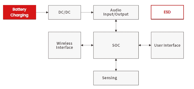
Smart Watch Circuit Protection Reference Block Diagram
PCB and EMC Design Considerations
1. Proximity to Interfaces: Whether it's the charging port or the data/button interface, these protective devices should be placed as close to the external interface as possible. This shortens the path of electrostatic discharge or surge current into the circuit board.
2. Good Grounding: The grounding path of the protective devices must be short and wide, directly connected to the main ground plane. If the grounding path is too long or too narrow, parasitic inductance will be generated, leading to poor discharge.
Conclusion
With over 15 years of EMC protection expertise, Semiware provides comprehensive circuit protection solutions including TVS diodes, ESD devices, and circuit-level protection support for wearable electronics.
If you are designing Smart Watches or wearable devices, contact Semiware for circuit protection solutions and component selection support.