Overview
In applications such as NFC antennas, portable electronic devices, and other circuits requiring high signal integrity, ESD protection devices must not only meet electrostatic protection standards but also balance factors such as device capacitance, leakage current, clamping characteristics, and PCB space constraints.
The SE06F10B18UA is a single-channel, bidirectional ESD protection diode from Semiware. Housed in a compact DFN0603 package, it features a reverse working voltage of 18V and a typical junction capacitance of 0.5pF, making it specifically designed for ESD protection in high-frequency signal lines.
Additionally, the Nexperia PESD18VF1BSF is also suitable for NFC antenna protection; for engineers and procurement professionals seeking an alternative solution, Semiware’s SE06F10B18UA is a compelling option worth considering.
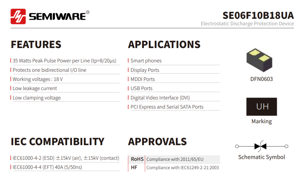
I. SE06F10B18UA Specifications
The SE06F10B18UA is a bidirectional ESD protection device for single signal lines. Key specifications are as follows:
- Device Type: Low-capacitance TVS diode
- Reverse Working Voltage (VRWM): 18 V
- Breakdown Voltage (VBR): 19 V (min), 22 V (typ) @ IT = 1 mA
- Junction Capacitance (CJ): 0.5 pF (typ)
- Reverse Leakage Current (IR): 0.2 μA (max) @ VRWM = 18 V
- Peak Pulse Power (PPP): 35 W (8/20 μs)
- ESD Protection Rating: IEC 61000-4-2; Contact Discharge ±15 kV, Air Discharge ±15 kV
- Package: DFN0603-2L
- Operating Temperature Range: -40°C to +125°C
II. Key Features of the SE06F10B18UA
2.1 Bidirectional ESD Protection
The SE06F10B18UA features a bidirectional TVS structure capable of rapidly discharging both positive and negative ESD surges. It is suitable for NFC antennas, differential signals, and AC signal lines, without the need to consider signal polarity.
2.2 Small Package, Ideal for Compact PCB Designs
The DFN0603-2L package is suitable for electronic products with limited PCB space.
2.3 Low Capacitance
With a typical junction capacitance of 0.5 pF, the device balances ESD protection with RF performance when integrated into a circuit, ensuring signal integrity remains unaffected.
2.4 Low Leakage Current (μA Range)
The leakage current is 0.2 μA at an operating voltage of 18 V, making it suitable for high-impedance signal paths. Its low static power consumption prevents signal baseline drift.
2.5 Complies with RoHS lead-free environmental standards and meets environmental requirements for consumer electronics and IoT products.
III. Key Applications of the SE06F10B18UA Low-Capacitance ESD Diode
Based on the specifications and characteristics outlined above, the SE06F10B18UA low-capacitance ESD diode is primarily used in:
- NFC antennas and associated signal lines
- Portable consumer electronics
- Compact IoT modules
- Other signal lines requiring single-channel, bidirectional ESD protection
IV. Why is the SE06F10B18UA a Suitable Replacement for the Nexperia PESD18VF1BSF?
As mentioned at the beginning of this article, the Semiware SE06F10B18UA serves as a potential replacement for the Nexperia PESD18VF1BSF. The following section provides a detailed analysis of the key factors for evaluating this replacement.
4.1 Parameter Comparison
| Parameter | SE06F10B18UA | PESD18VF1BSF |
| VRWM | 18V | 18V |
| VBR | 19V | 19V |
| CJ | 0.5 pF typ | 0.28 pF typ |
| Contact Discharge ESD | ±15 kV | ±10 kV |
| Air Discharge ESD | ±15 kV | ±15 kV |
| IR | 0.2 μA | 1 nA |
| Package | DFN0603-2L | DFN0603-2L |
4.2 Replacement Analysis
The parameter comparison above shows that the SE06F10B18UA and PESD18VF1BSF are compatible in terms of operating voltage, ESD rating, and package type. Although there are slight differences in capacitance values as listed in the datasheets, engineering batch verification can be conducted to confirm suitability for replacement.
Datasheets and Samples
If you are evaluating the SE06F10B18UA, contact Semiware for the product datasheet, samples, and selection support.