Overview
As "lightning and ESD protection experts" in the electronics industry, our responsibility is not merely to provide simple switching protection for circuits, but rather, like meticulous structural engineers, to build a circuit "defense system" on the PCB board that neither interferes with signal transmission nor instantly deflects kilovolt-level electrical hazards.
The diodes, varistors, and other small black components on the PCB board may seem insignificant, but in actual engineering environments, they are the only "armor" protecting electronic devices from external electrical interference.
I. Why Do Electronic Devices Need "Armor" Protection?
- External Core Threats
Electrostatic discharge (ESD) generated when a person touches the device interface (compliant with IEC 61000-4-2 standard) and lightning surges on power lines (compliant with IEC 61000-4-5 standard) can instantly puncture the oxide layer of delicate back-end chips such as CPUs and LDOs, causing device damage.
- Semiware Core Insights
Without the "armor" of protective devices, electronic equipment is not only highly susceptible to catastrophic damage, but also frequently experiences stability issues such as packet loss and system crashes in complex electromagnetic environments, rendering it unable to function properly.
II. Core Terminology Explanation: Capacitors and Clamping Voltages
Selection parameters are among the most frequently asked questions by FAE engineers. For beginners in circuit protection, understanding the engineering trade-offs behind these two "golden indicators"—capacitors and clamping voltages—is essential; it forms the foundation of device selection.
- Capacitor (Cj)
Capacitors directly determine the degree of influence of protective devices on signal waveforms. In high-speed signal scenarios such as 40Gbps USB 4 and 10G Ethernet, the high parasitic capacitance of devices can cause severe insertion loss, leading to eye diagram closure and ultimately communication failure. Therefore, protection devices for high-speed signal lines must achieve extremely low capacitance, around 0.2pF.
- Clamping Voltage (VC)
VC is a core indicator of the protection efficiency of devices. It refers to the actual voltage at which the device can be effectively controlled when electrical interference occurs. If VC exceeds the breakdown voltage of the downstream chip, even if the protection device itself is not damaged, the delicate downstream chip will be broken down and destroyed.
III. Signal Protection vs. Power Protection
In circuit protection design, appropriate protection devices must be selected based on the needs of these two different "battlefields": signal protection and power protection. Their design logic and selection criteria differ fundamentally:
- Different Success Indicators
Signal protection prioritizes extremely low capacitance to ensure the "transparency" of signal transmission and prevent additional interference; power protection, on the other hand, pursues high peak pulse current withstand capability (IPP) to achieve efficient surge current discharge.
- Different Circuit Layouts
Signal protection devices are typically connected in parallel between the signal line and ground, requiring extremely streamlined wiring to reduce signal loss; power protection serves as a powerful surge discharge channel, sometimes requiring the use of inductors and PPTCs to form a "multi-level collaborative" protection structure.
- Different Failure Consequences
Failure of signal protection devices typically manifests as functional problems such as data errors and system crashes; failure of power protection devices often leads to serious malfunctions such as hardware burnout and equipment failure.
IV. Practical Protection Case Studies: Device Selection and Layout Guidelines for Different Scenarios
Case Study 1: Multi-Level Defense for USB Interfaces
USB interfaces are the primary channel for electrostatic discharge (ESD) intrusion into electronic devices. The selection logic for protective devices differs significantly for USB interfaces with different transmission rates, requiring precise matching.
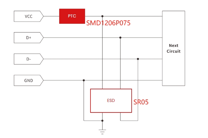
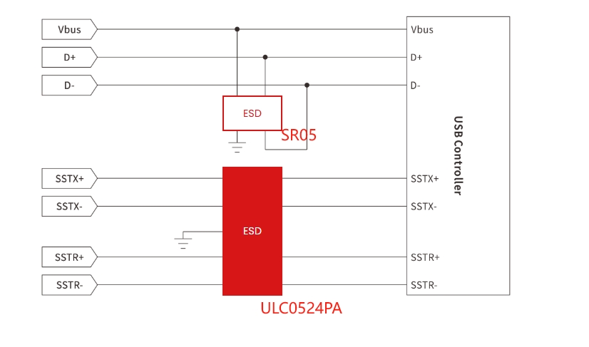
- USB 2.0 Protection: The SR05 TVS array is recommended, featuring low capacitance, good channel symmetry, and sufficient ESD protection capabilities. It effectively protects the interface without affecting the integrity of high-speed signals.
2. USB 3.0/Type-C Protection: For high-speed signals above 5Gbps, the ULC0524PA in a DFN2510 package is recommended. It features ultra-low capacitance (0.6pF), high ESD rating (±15kV), and USB 3.0 differential high-speed compatibility, without affecting 5Gbps signal transmission.
USB Interface Layout Guidelines:
ESD protection devices must be placed close to the connector interface, following the "discharge nearby" principle. Static electricity must be eliminated locally before it enters the core area of the PCB, preventing induced noise from coupling into internal circuitry.
Case Study 2: Precise Protection of SIM Cards and Buttons
SIM card protection is a typical space-constrained scenario. Multiple pins, including I/O, Clock, and Reset, need simultaneous protection. The core design principle is "integration, small size, and high standards."
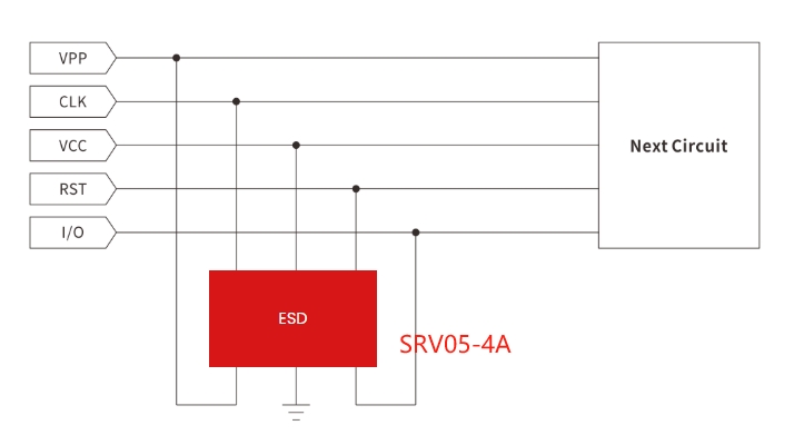
- Integrated Protection Selection:
The SRV05-4A (SOT-26 package) is selected. A single device can achieve full coverage protection for 4-5 pins, significantly saving PCB space.
- Performance Verification Standards:
Protection devices must meet IEC61000-4-2 Level 4 standards (contact 8kV / air 15kV); simultaneously, the device capacitance must be controlled to avoid excessive capacitance causing signal edge slowing, affecting normal device operation.
V. Four-Step Method for Selecting Protective Devices
- Confirm Operating Voltage (V_RWM):
This is the device's "cutoff voltage." At this voltage, the device must remain "transparent" and free from conduction interference. When selecting a device, V_RWM must be greater than the circuit's maximum operating voltage (e.g., select a 5V device for a 5V rail, not a 3.3V device, otherwise it may cause misconduct).
- Match Package and Space:
Select a device based on the actual PCB space. For high-speed lines, the DFN2510 through-hole package is preferred; for power lines, SMC or high-power SMB packages are preferred.
- Compare with Testing Standards:
Select a device based on the required testing levels for the product. Determine the electrostatic discharge protection level according to IEC 61000-4-2 (ESD) standard, and determine the device's I_PP power according to IEC 61000-4-5 (Surge) standard.
- Check residual voltage (VC):
Ensure that the clamping voltage (VC) of the protection device is lower than the damage voltage of the downstream chip to form effective protection.
👉 Need a reliable ESD/TVS solution that meets both technical requirements and cost targets?
Contact us for customized recommendations, fast delivery samples, and pricing support tailored to your project. https://en.semiware.com/contact/


Comments (0)