I. What is a MIPI Interface?
MIPI (Mobile Industry Processor Interface) is a high-speed interface specification designed for mobile and embedded devices, commonly used for data transmission between processors and components such as cameras and displays. Compared to traditional parallel interfaces, MIPI employs high-speed serial differential transmission, enabling high data bandwidth with fewer pins.
 ESD-Protection-Design-for-MIPI-Interfaces.jpg" alt="ESD Protection Design for MIPI Interfaces: Component Selection and Layout for High-Speed Differential Signals" title="ESD Protection Design for MIPI Interfaces: Component Selection and Layout for High-Speed Differential Signals" alt="" class="wp-image-18809" style="width:615px;height:auto"/>
II. What Are the Characteristics of MIPI Circuits?
- High-Speed Differential Signals
MIPI data channels typically utilize differential signal transmission. While the differential structure inherently enhances noise immunity and reduces EMI, high-speed differential lines are sensitive to PCB trace characteristics and parasitic parameters.
- Fast Signal Edge Rates
MIPI operates at high data rates; rapid signal transitions imply the presence of high-frequency harmonic components. Consequently, low-capacitance ESD devices are prioritized for high-speed MIPI lines.
- Low Signal Voltage
MIPI interfaces operate in a low-voltage, high-speed signal environment, requiring careful selection of the ESD device's operating voltage and clamping voltage.
III. What ESD Risks Do MIPI Interfaces Face?
Although MIPI interfaces are typically located inside the device, areas such as camera modules, display modules, FPCs (Flexible Printed Circuits), and connectors can serve as entry points for electrostatic coupling or conduction.
3.1 Direct External Electrostatic Coupling
When a user touches the device casing, connectors, or modules, human-body static electricity can couple into the MIPI signal channels via structural components, FPCs, or interface lines.
3.2 ESD Paths via FPCs
Cameras and displays frequently use FPC connections. These FPCs are often long and positioned near the device edges, allowing their signal lines to act as pathways for static electricity to enter the mainboard.
3.3 Direct ESD Entry into SoC/ISP
Without external protection devices on the MIPI signal lines, ESD transients can propagate directly along the lines into the system.
IV. Semiware MIPI ESD Protection Solutions
Semiware’s MIPI reference solutions primarily utilize low-capacitance ESD diodes and multi-channel TVS arrays, selected specifically to meet the low parasitic capacitance requirements of high-speed differential MIPI signals.
Test Standards:
IEC 61000-4-2: Contact ±8 kV; Air ±15 kV
Reference Block Diagram:
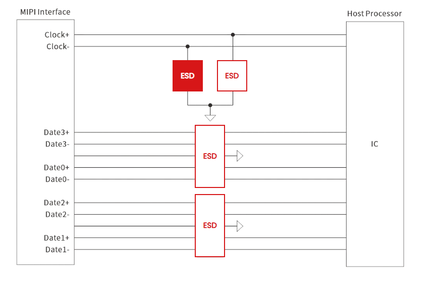
For MIPI high-speed differential links, Semiware offers multi-channel ESD diodes utilizing ultra-low junction capacitance technology. These devices balance ESD discharge capability with high-speed signal integrity; the parameters for devices suitable for MIPI projects are listed below.
| Part Number | Package | Working Voltage (VRWM) | ESD Protection | Typical Capacitance |
| SE06F10B3.3MA | DFN0603-2L | 3.3 V | ±18 kV | 0.28 pF |
| SE10F10B3.3MA | DFN1006-2L | 3.3 V | ±23 kV | 0.22 pF |
| SEULC3304P | DFN2510-10L | 3.3 V | ±30 kV | 0.40 pF |
V. MIPI PCB Layout and Routing Guidelines
Place ESD protection">ESD protection devices as close as possible to the FPC or board-to-board connector to shunt electrostatic discharge (ESD) to ground immediately upon entry, thereby shortening the discharge path and minimizing parasitic inductance.
Connect the GND pin of the ESD device directly to the solid ground plane using a short, wide trace; avoid long, thin, or meandering ground traces.
Strictly control trace length matching and impedance for MIPI differential pairs; place ESD devices on the connector side rather than inserting them in the middle of the differential lines, which would create a branch.
Group multiple MIPI lanes together during layout to ensure that parasitic characteristics remain as consistent as possible across all differential pairs.
Learn more about Semiware's MIPI ESD protection">ESD protection reference designs: