Overview
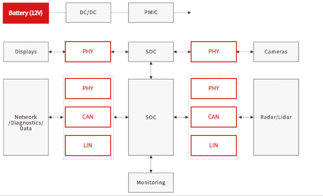
External cameras support ADAS functions such as lane departure warning, while internal cameras enable eye tracking to help prevent accidents caused by driver drowsiness. In addition to protection against common electrical threats, data communication buses require safeguards that do not interfere with high-frequency video signals. Semiware’s solutions include TVS diodes, ESD suppressors, Schottky diodes, and resettable fuses.
I. Application Framework
II. Load Dump Protection
Load dump protection at the power input follows a clear, hierarchical approach: dissipate, clamp, and—if necessary—disconnect.
- A fuse is typically used in conjunction with a TVS diode. If a TVS diode absorbs an excessively high-energy pulse or fails (short-circuits due to degradation), it may create a continuous current path. A series fuse (or e-fuse) will then break the circuit, preventing thermal runaway from spreading.
- For more demanding load dump requirements or applications requiring higher integration, a load switch or an ideal diode controller can be used alongside an external TVS diode. These components can actively disconnect or limit the current path during a surge, isolating downstream circuitry from transient energy. They also integrate overvoltage, overcurrent, and reverse-polarity protection, thereby reducing the component count and the required PCB footprint.
- An LC filter circuit serves as a final “refining” stage after the initial energy dissipation, smoothing out residual voltage fluctuations and ringing, and reducing the stress placed on downstream power management ICs by high-frequency transients.
III. ESD Protection
- The challenge in ESD protection lies not in the ability to clamp voltage, but in doing so without compromising signal integrity. High-speed ADAS interfaces are extremely sensitive to parasitic capacitance; therefore, the selection of protection components must be based on the specific data rate and impedance requirements of the interface.
- For CAN/CAN FD buses, transceivers are directly exposed to vehicle wiring harnesses and connectors, making them a primary entry point for ESD. Protection is typically implemented using bidirectional TVS diodes, connected between the CANH/CANL lines and ground. A key constraint is that junction capacitance must not significantly affect the differential signal. Although the data rate of CAN FD is much lower than that of Ethernet, the combination of common-mode chokes and TVS diodes still requires careful control of parasitic parameters. Leimao’s solution ensures that the clamping voltage remains below the module’s maximum withstand voltage (typically around 45V) while meeting the ±25 kV air-discharge requirement specified by the ISO 10605 Level 4 standard. Similarly, the TPSE23T20B24LB series recommended by Semiware is designed to provide the necessary level of protection without introducing excessive capacitive loading.
- The constraints for automotive Ethernet (100/1000BASE-T1) are even more stringent. For 100BASE-T1, the junction capacitance of an ESD protection device must be ≤1 pF, while for 1000BASE-T1, this limit is tightened further to ≤0.5 pF. Exceeding these values would disrupt the impedance matching of the differential pair, leading to the closure of the signal eye diagram. In terms of component selection, the ESD5E002TA—with a junction capacitance (Cj) of only 0.18 pF—is a typical choice for Gigabit automotive Ethernet. Regarding layout, the ESD device must be placed as close as possible to the PHY pins, with trace lengths kept under 5 mm to minimize the protection loop and prevent parasitic inductance from compromising the clamping performance.
- For the RF front-end of millimeter-wave (mmWave) radar (77/79 GHz), there is virtually no margin for external ESD components. The ESD withstand capability of the RF chip pins themselves is only 100–500V; however, any additional PCB-level protection component with a junction capacitance exceeding approximately 0.15 pF would severely disrupt 77 GHz impedance matching. Consequently, ESD protection for mmWave RF ports relies primarily on on-chip integration, with no discrete components placed on the PCB. At the system level, the focus shifts toward electrostatic control during the assembly process, proper connector grounding, and module shielding.
- For camera links (such as FPD-Link), ESD performance is a system-level consideration. TI’s application notes explicitly state that chip-level ESD ratings (HBM, CDM) found in datasheets cannot be directly equated to application-level performance. While a chip itself may remain “undamaged,” the data link could still experience data loss or latch-up during an ESD event. An effective strategy involves a hardware-software co-design approach: optimizing connector grounding and the PCB-to-enclosure ground path in hardware, while utilizing latch-up detection, tuning, and Forward Error Correction (FEC) in software to tolerate transient bit errors. This combined approach ensures that the system meets the stringent ESD requirements set by OEMs.
IV. System-Level Layout
Regardless of how precisely components are selected, poor return-path design will significantly undermine protection effectiveness. ESD current seeks the path of least impedance to ground; therefore, connector ground pins should be connected directly to a solid, large-area ground plane. It is also essential to ensure that this plane is linked to other ground planes on the board via vias or connectors, creating a low-inductance path. Metal enclosures, shielding, and external sensor structures must be reliably bonded to the PCB ground, directing discharge currents to the chassis ground before they can reach sensitive circuitry. For interfaces involving long wire harnesses—such as those for automotive radar or camera systems, which can span 3 to 5 meters—long cables can exacerbate ESD coupling. In such cases, a front-end topology combining a common-mode choke with a TVS (Transient Voltage Suppressor) diode is commonly employed.
V. Usage Considerations
- ESD suppressors must be placed as close as possible to the LIN physical interface (connector) to provide the fastest discharge path.
- Zener diodes should not be used as substitutes for dedicated ESD suppressors (as they offer slower response times and inferior clamping capabilities).
- The presence of built-in protection within a LIN transceiver does not eliminate the need for external protection components.
- An optional RC filter may be added (to limit slew rate and suppress spikes)—for example, using R=100Ω and C=1nF to 2.2nF (exercise caution, as excessive values may interfere with communication).
Learn More
For further information on circuit protection solutions and applications for automotive lighting (headlights) and related systems, please visit: https://en.semiware.com/applications/adas/

评论 (0)