📌 Overview
The 12N65F is a common 650V high-voltage MOSFET specification used in off-line switching power supplies; it is widely applied in power conversion systems such as industrial power supplies, LED drivers, AC-DC power supplies, and PFC circuits. To address challenges regarding the lead times, costs, and supply stability of imported components, engineers and procurement teams require alternative solutions that balance electrical performance, package compatibility, and supply chain reliability.
The Semiware SNMF12N65 is a 650V N-channel enhancement-mode planar VDMOS MOSFET housed in an insulated TO-220F package, specifically designed for 12N65F-class applications. It features an optimized balance between RDS(on), gate charge, and avalanche ruggedness, making it suitable for both new project selection and as a drop-in replacement for existing BOMs; for designs utilizing the compatible TO-220F package and pin configuration, verification can typically be performed without modifying the PCB layout.
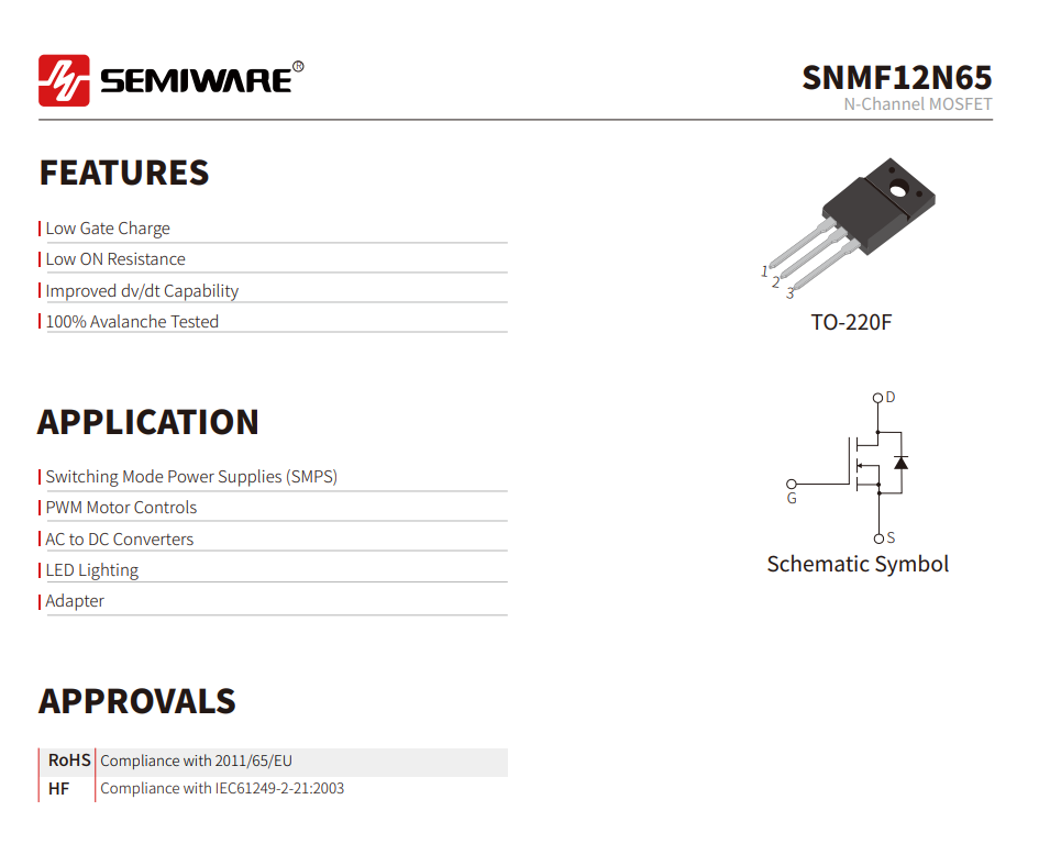
📌 Key Electrical Parameters of the SNMF12N65 MOSFET
| Parameter | SNMF12N65 |
| Drain-Source Voltage | 650 V |
| Continuous Drain Current | 12 A @ 25°C |
| Pulsed Drain Current | 40A |
| Gate-Source Voltage | ±30 V |
| Drain-Source On-State Resistance | 0.65 Ω Typ |
| Total Gate Charge | 38 nC Typ. |
| Single-Pulse Avalanche Energy | 576 mJ |
| Operating Junction Temperature | −55 to +150°C |
📌 SNMF12N65 MOSFET Key Features
- Insulated TO-220F Package: Utilizes the industry-standard TO-220F package configuration, facilitating replacement evaluations for 12N65F-class devices; simplifies heatsink mounting while meeting mechanical and safety requirements.
- Optimized On-Resistance: RDS(on) of 0.71Ω (Typ.) helps reduce conduction losses and manage device heat generation during high-power operation.
- Balanced Gate Charge and Switching Performance: Total gate charge of 48nC (Typ.) strikes a balance between conduction and switching losses, making it suitable for design evaluation in hard-switching topologies such as flyback converters and PFC boost stages.
- Robust Avalanche Capability: Single-pulse avalanche energy (EAS) of 790mJ with 100% avalanche testing provides additional design margin against transient voltage stresses caused by transformer leakage inductance and parasitic parameters.
- Wide Operating Junction Temperature Range: -55°C to +150°C, suitable for applications with varying ambient temperature requirements, such as consumer electronics and industrial power supplies.
- RoHS Compliance: Meets relevant environmental requirements; suitable for the design of electronic products for the global market.
📌 Typical Application Scenarios for the SNMF12N65 MOSFET
The SNMF12N65 is designed for high-voltage offline power supplies and power conversion applications. Selection should be based on specific factors such as topology, input voltage, switching frequency, load power, and thermal management requirements.
Key applications include:
- AC-DC Switching Power Supplies: Industrial adapters, high-power chargers, internal power supplies for industrial PCs, etc.
- PFC (Power Factor Correction) Circuits: Suitable for MOSFET selection in boost PFC power stages.
- High-Power LED Drivers: Constant-current drivers for lighting equipment such as LED streetlights and industrial high-bay lights.
- UPS and High-Voltage DC-DC Conversion: Small UPS units, high-voltage DC-DC conversion modules, and auxiliary power supplies.
- Power Supplies for Home Appliances and Industrial Equipment: Power boards for high-power home appliances and auxiliary power units for industrial equipment.
📌 Engineering Design Considerations and Recommendations
- Voltage and Current Derating: It is recommended to keep the actual operating voltage within 80% of the VDSS rating. Do not use the datasheet's rated current (specified at 25°C) as the continuous system operating current; significant current derating is required for high-temperature operating conditions.
- Thermal Design: Although the TO-220F package features built-in insulation, adequate heat dissipation area is still required to control the junction temperature and prevent overheating failures during prolonged full-load operation.
- Gate Drive Settings: A Vgs of 10V is recommended to achieve optimal on-resistance (Rds(on)). Do not leave the gate pin floating; adding a pull-down resistor is recommended to prevent accidental turn-on. Existing gate resistors can be retained, but if testing reveals excessive switching noise, the gate resistor (Rg) value can be moderately increased to suppress oscillation.
- Snubber Circuits: For flyback and PFC circuits, retaining an RC snubber circuit is recommended to suppress voltage spikes caused by transformer leakage inductance and to reduce voltage stress on the MOSFET.
For complete electrical parameters and test curves, please refer to the official Semiware datasheet:
Summary
When selecting 650V high-voltage MOSFETs for off-line power supply designs, one must consider not only basic electrical parameters but also switching performance, thermal design, package compatibility, and long-term supply availability. For projects currently utilizing 12N65F-series devices, the SNMF12N65 is a viable alternative worth evaluating.
Before actual implementation, it is recommended to verify the device against the original component's datasheet, operating waveforms, PCB thermal conditions, and system-level reliability requirements. Semiware provides datasheets, samples, and FAE technical support to assist engineering teams with component selection and substitution evaluation.