I. What is Electrostatic Discharge (ESD)?
Electrostatic discharge (ESD) is the instantaneous transfer of charge between two objects with different electrical potentials.
For example, the "electric shock" felt when touching a doorknob in winter is a typical ESD phenomenon.
In electronic systems, the ESD voltage on the human body can reach thousands of volts, while the gate oxide layer of modern chips is only nanometers thick, making it extremely easy to break down and damage.
II. How is Static Electricity Generated?
Static electricity essentially originates from charge transfer. When two different materials come into contact, rub, or separate, such as when plugging and unplugging a USB cable or when a plastic casing rubs against each other, electrons are transferred. The greater the difference in position of the materials in the "triboelectric sequence," the higher the electrostatic voltage generated.
III. Why is ESD Protection Becoming Increasingly Important?
The miniaturization of conductor devices is a double-edged sword:
1️⃣ On the one hand, as semiconductor processes enter 7nm, 5nm, and even more advanced nodes, device sizes continue to shrink.
According to scaling principles: when the size shrinks to 1/k, the area shrinks to 1/k², and power consumption and latency decrease simultaneously.
2️⃣ On the other hand, the SiO₂ insulating layer is simultaneously thinned, while the dielectric strength remains constant at approximately 8–10 MV/cm.
➡️ Result: The dielectric withstand capability of the insulating layer decreases, and ESD sensitivity increases significantly.
3️⃣ Furthermore:
- Frequent plugging and unplugging of interfaces such as USB/Type-C;
- High device integration;
- Increased automation in production environments
all further increase ESD risks.
Therefore, ESD protection">ESD protection has become an essential component of electronic design, with TVS diodes being one of the most mainstream solutions.
IV. Device-Level ESD Testing Standards
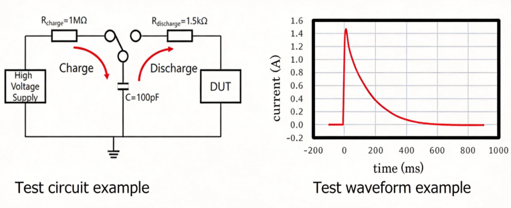
- Human Body Model (HBM): Simulates discharge when a worker makes live contact with a chip.
Standard: JEDEC JESD22-A114, 2kV–8kV
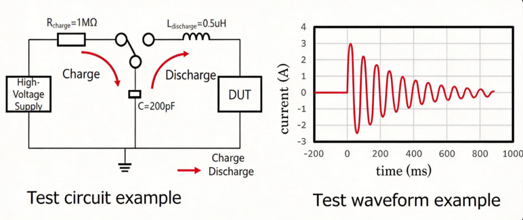
- Machine Model (MM): Simulates discharge when automated equipment (e.g., a pick-and-place machine) makes live contact with a device.
Standard: JEDEC JESD22-A115, faster and stronger discharge current.
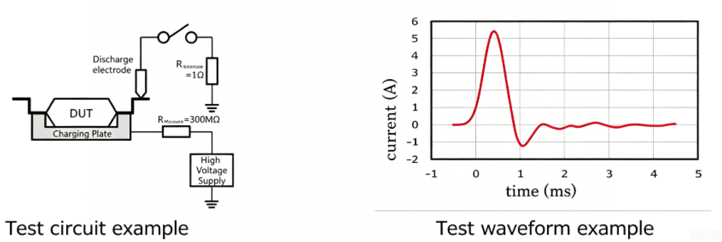
- Charged Device Model (CDM): Simulates discharge when a self-charged chip contacts a grounded circuit board.
Standard: JEDEC JESD22-C101, tests the device's instantaneous impact resistance.
V. System-Level ESD and Surge Testing
IEC 61000-4-2 (System ESD Testing):
- Contact Discharge: ±8kV (Conventional Industrial Requirements)
- Air Discharge: ±15kV (Typical Requirements)
- Semiware ESD devices can achieve ±30kV immunity.
IEC 61000-4-5 (Surge Testing):
- Simulates Lightning Strike and Switching Surge
- Waveform: 8/20μs
- Peak Current Up to 100A or More (High-Power Devices)
VI. Semiware ESD Protection Solutions
Common protection devices include:
Semiware provides complete ESD protection">ESD protection solutions covering:
- USB Type-C / HDMI Interfaces
- Automotive Electronic Systems
- Industrial Control Equipment
- IoT and Consumer Electronics
Summary
Although ESD is invisible, it can be highly destructive to electronic systems. Especially with the miniaturization and high-frequency operation of electronic devices today, protection has become a necessity.
Looking for an ESD protection">ESD protection solution for your application? Contact the Semiware team for product recommendations, technical support, or samples.


Comments (0)