Introduction
In electronic systems, electrostatic discharge (ESD), surges, and electrical transient interference can often cause irreversible damage to chips within an extremely short timeframe.
To address these issues, two core types of protection devices are commonly used in engineering:
ESD Diodes: Primarily used for electrostatic protection (nanosecond-scale transients); suitable for high-speed signal interfaces and low-voltage circuits.
TVS Diodes: Primarily used for surge protection (microsecond- to millisecond-scale energy surges); suitable for power supplies and industrial/automotive systems.
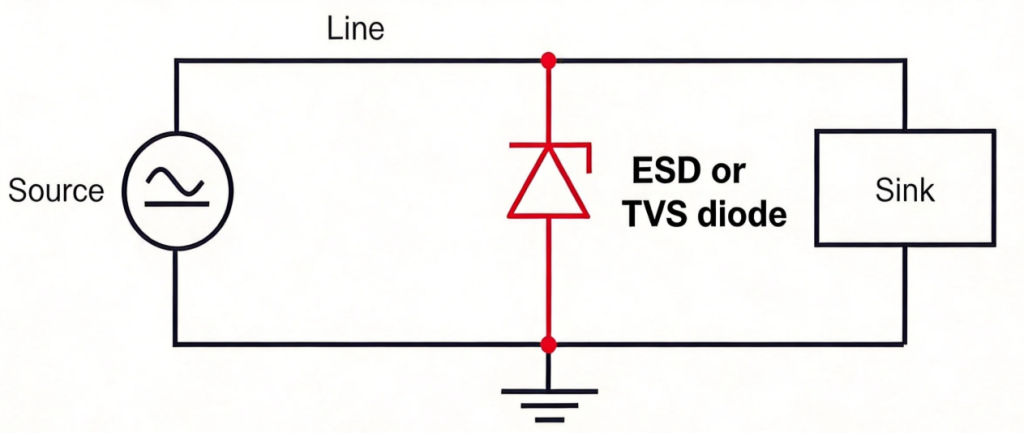
In practical designs, both are typically connected in a "parallel clamping" configuration to signal or power lines to dissipate transient energy.
I. ESD vs. TVS: Fundamental Differences
| Item | ESD Diode | TVS Diode |
| Purpose | Electrostatic protection | Surge protection |
| Energy Level | Low energy, fast event | High energy surge |
| Response Time | ns level | ns level |
| Typical Use | USB / HDMI / GPIO | Power / Industrial / Automotive |
| Standards | IEC 61000-4-2 | IEC 61000-4-5 |
👉 ESD diodes guard against "fast transients," while TVS diodes withstand "high energy."
II. Key Selection Parameters
- VRWM (Reverse Working Voltage)
VRWM determines whether the device triggers "false operation" during normal working conditions.
| Protection Type | Operating Voltage | Recommended VRWM |
| ESD Protection | 3.3V | ≥3.3V |
| ESD Protection | 5V | ≥5V |
| ESD Protection | 12V | ≥12V |
| Surge Protection (IEC 61000-4-5) | 5V | ≥6V |
| Surge Protection (IEC 61000-4-5) | 12V | ≥15V |
| Surge Protection (IEC 61000-4-5) | 24V | ≥26V |
| Automotive (ISO 7637-2 / Load Dump) | 12V | ≥22V |
| Automotive (ISO 7637-2 / Load Dump) | 24V | ≥30V |
| Automotive (Load Dump / EV Systems) | 48V | ≥58V |
👉 VRWM ≥ 1.2 × Maximum System Operating Voltage
- Clamping Voltage VC (The key to "successful protection")
VC must be lower than the withstand voltage of the chip being protected; otherwise, the protection is ineffective.
| Item | Description |
| Definition | Voltage during surge clamping |
| Design Rule | VC must be lower than IC absolute max rating |
| Key Factor | Higher IPP → higher VC |
👉 It is not a question of "whether it conducts," but rather "to what level the voltage is clamped."
- Parasitic Capacitance CJ (Critical parameter for high-speed signals)
| Interface | Recommended CJ |
| GPIO / Button | <30 pF |
| Audio | <10 pF |
| USB 2.0 | <2.5 pF |
| USB 3.0 | <0.5 pF |
| USB 3.1+ | <0.3 pF |
| HDMI 2.0 | <0.5 pF |
| Ethernet | <5 pF |
| RF Antenna | <0.2 pF |
👉 Parasitic capacitance must meet signal integrity requirements.
- Surge Capability IPP (Energy withstand capability)
| Standard | Waveform | Application |
| IEC 61000-4-2 | ESD | Electrostatic discharge |
| IEC 61000-4-5 | 8/20 μs | Lightning surge |
| ISO 7637-2 | 10/1000 μs | Automotive transient |
| Load Dump | ms-level | Alternator load dump |
III. Selection Process
Step 1: Determine the application scenario:
- Signal or Power Supply
- Consumer Electronics / Industrial / Automotive
- Compliance with IEC surge testing standards
Step 2: Determine key parameters:
- VRWM
- VC
- CJ
- IPP
Step 3: Determine package and power rating:
- Small signal: DFN / SOD
- Power level: SMC / SMB
IV. Application Examples
Case 1: USB 3.0 ESD Protection (Consumer Electronics)
| Line | Device | Key Parameter |
| VBUS | SE10F10B5.0A | DFN1006-2L ,VRWM=5V, VC≈10V |
| D+/D- | SE10P3F10U5.0MB | DFN1006-3L, CJ≈0.6pF |
| SSTX/SSRX | ULC0524P | DFN2510, CJ≈0.3pF |
Case 2: 12V Industrial Power Surge Protection
Consumer Electronics:
| Item | Specification |
| Recommended Devices | SD12C / SE16F200U12A |
| Package | SOD-323/DFN1610-2L |
| ESD Standard | IEC 61000-4-2 Level 4 |
| Air/Contact Discharge | ±30 kV/±30 kV |
| Surge Capability | IEC 61000-4-5 (Lightning) |
Industrial Equipment:
For devices such as PLCs, sensors, and communication base station power modules, it is generally recommended that the TVS diode's VRWM be greater than 1.2 times the power supply voltage (e.g., SMBJ15CA). This prevents frequent false triggering of the TVS caused by voltage fluctuations in the power supply itself.
Conclusion
ESD and TVS diode selection is ultimately a balance between three key engineering requirements:
- Ensuring normal operation without false triggering (VRWM selection)
- Providing effective transient suppression (clamping capability, VC)
- Maintaining signal and system integrity (parasitic capacitance, CJ)
Different applications place different priorities on these parameters.
High-speed interfaces prioritize low capacitance, while power and industrial systems focus more on surge handling capability and clamping performance.


Comments (0)