Overview
Label printers are widely used in sectors such as retail, warehousing, logistics, and industrial manufacturing. These devices often require frequent plugging and unplugging of power and data cables, and some models also support Ethernet or Bluetooth connectivity.
During product testing or field operation, engineers may encounter issues such as printing anomalies, communication interruptions, unexpected device resets, or even damage to interface chips. Beyond software-related factors, transient disturbances—specifically Electrostatic Discharge (ESD), Electrical Fast Transients (EFT), and power surges—are critical causes that must be addressed.
Implementing a robust circuit protection design helps mitigate these risks, enhancing the operational reliability of label printers in complex electrical environments.
I. Which Circuits in a Label Printer Are Most Vulnerable to Transient Damage?
Transient protection for label printers primarily focuses on three areas: the power input, the printhead drive circuitry, and external communication interfaces.
- Power Input Circuitry
Plugging or unplugging the power supply, as well as fluctuations in the external power source, can introduce transient overvoltages. Furthermore, the switching of pulsed currents to the printhead can cause power supply instability, potentially affecting the power management IC and the main control circuitry.
- Printhead Drive Circuitry
The pulsed currents and switching actions that occur during printhead operation can generate electrical noise and transient voltages. If this interference couples into sensitive components or other power rails, it may compromise printing stability—or, in severe cases, cause component damage.
- External Communication Interfaces
Interfaces such as USB, RS-232, and Ethernet are vulnerable to ESD strikes during connection or disconnection. This can lead to communication failures, device resets, or damage to interface chips. Consequently, appropriate protection circuits should be designed based on the specific characteristics and immunity requirements of each interface.
II. Circuit Protection Design for Label Printers
Designing protection for label printers requires a comprehensive approach: considering power characteristics, interface types, and potential transient risks to select suitable protection components, while also accounting for signal integrity and PCB layout.
2.1 Selection of Protection Components
Semiware offers Transient Voltage Suppressor (TVS) diodes and ESD protection diodes, which can be utilized to provide transient voltage protection across various circuit sections.
a. TVS Diodes: Suitable for transient overvoltage protection on power lines, provided they meet the device's specific requirements. Key parameters to consider during selection include operating voltage, clamping voltage, and peak pulse power.
b. ESD Protection Diodes: Primarily used for electrostatic discharge (ESD) protection on external communication interfaces. For high-speed interfaces such as USB or Ethernet, parasitic capacitance must be carefully managed to avoid compromising signal integrity.
When selecting protection components, ensure they can withstand the anticipated transient conditions and keep the voltage stress on the protected ICs within their rated limits.
2.2 Protection Schemes for Various Circuit Modules
a. Power Input:
A suitable TVS diode can be placed at the power entry point to suppress transient overvoltages, potentially combined with filtering circuitry if necessary. For printhead drive circuits, the necessity for additional suppression measures should be evaluated based on the source and propagation path of switching transients.
b. Communication Interfaces:
USB: Low-capacitance ESD protection arrays can be used for D+ and D− signal lines; the VBUS line should be evaluated separately based on specific requirements.
RS-232: Select protection components that accommodate the positive and negative signal voltage ranges and align with the voltage tolerance specifications of the transceivers.
Ethernet: Choose protection components based on the interface architecture, signal integrity requirements, and transient risks, while also considering the isolation transformer and grounding design.
Bluetooth / RF Interfaces: If protection for an antenna feed line is required, select low-capacitance components suitable for RF applications to prevent significant degradation of RF performance.
2.3 PCB Layout and Grounding
The placement of protection components directly impacts their effectiveness. Design considerations include:
a. Proximity to Interfaces: Place protection components as close to external connectors as possible to minimize the length of unprotected traces.
b. Optimized Discharge Paths: Reduce the length and parasitic inductance of the grounding paths for protection components, and ensure proper connection to the ground plane.
c. Control of Interference Coupling: Keep sensitive signals away from interfaces and PCB edges; also, consider the integration of chassis grounding and the overall return path during the design process.
III. Label Printer Reference Design Block Diagram
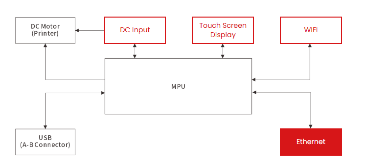
Learn more about circuit protection solutions for label printers: https://en.semiware.com/applications/label-printer/
Conclusion
Selecting appropriate protection components helps enhance product reliability. Please contact our team if you need data sheets or support with component selection.