Latch-up occurs when a parasitic structure within a CMOS device is "accidentally triggered," creating a positive feedback loop for current inside the chip. This current amplifies uncontrollably—like a flood—potentially burning out the chip or even crashing the entire power system.
I. How Does Latch-up Occur?
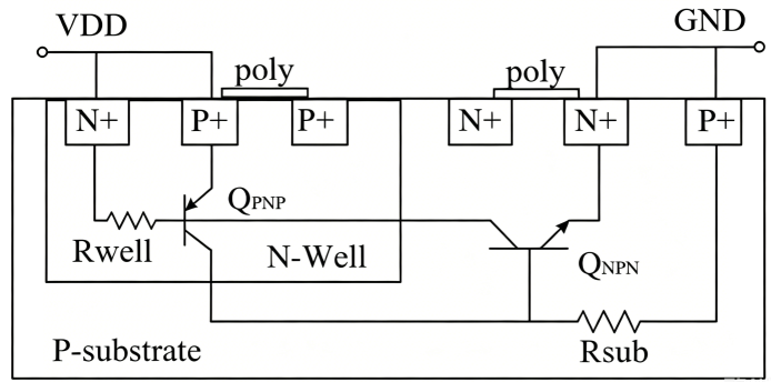
In CMOS fabrication, NMOS and PMOS structures are not entirely isolated; a parasitic PNPN structure (acting like an SCR thyristor) is formed between them.
Under normal conditions, this structure remains "dormant." However, it can be triggered by:
Electrostatic Discharge (ESD)
Voltage spikes (Surge)
Power supply fluctuations or transient disturbances
High-temperature environments
Once triggered, a positive feedback loop forms → current surges rapidly → the chip enters a state of "self-conduction."
👉 The result: Uncontrolled current + skyrocketing power consumption + abnormal chip heating or even burnout.
II. What Are the Typical Signs of Latch-up?
Be alert for the following symptoms, which may indicate a latch-up event:
- Sudden current surge (far exceeding normal operating levels)
- "Cliff-like" drop in supply voltage
- Chip resets, system freezes, or functional malfunctions
- Recurring failure, especially in high-temperature environments (particularly above 85°C)
III. How Can Latch-up Risks Be Detected?
Three main methods are typically used in engineering:
- ESD Testing
Simulates human-body electrostatic discharge (IEC 61000-4-2) to verify the chip's immunity to interference.
- Surge Testing
Simulates lightning strikes or power fluctuations (IEC 61000-4-5) to observe system stability.
- Simulation Analysis
Uses tools like TCAD to analyze the trigger threshold of the parasitic SCR structure, mitigating risk at the design stage.
IV. Latch-up Risks and Protection Strategies for Various Devices
- IGBT Power Devices
Risk Trigger: High-current surge (>10A)
Protection Strategies:
- Series current-limiting resistor
- Fuse protection
- Overcurrent shutdown circuit
👉 Recommended Products: Power protection TVS series
- CMOS / MCU / ASIC Chips
Risk Trigger:
I/O voltage exceeding limits (< -1.8V or > VCC + 0.7V)
Protection Strategies:
- I/O series resistor (approx. 200Ω)
- TVS diode clamping
- Reliable grounding design (ground-first connection for hot-swapping)
👉 Recommended Products: Low-capacitance ESD protection devices
- LDO Regulators
Risk Trigger: Output overcurrent or abnormal load
Protection Strategies:
- Current-limiting resistor
- Reset protection circuit
- Selection of latch-up-resistant models
- Operational Amplifiers
Risk Trigger: Output short circuit or overload
Protection Strategies:
- Output current-limiting resistor
- PPTC resettable fuse
👉 Recommended Products: PPTC resettable fuse series
V. Semiware System-Level Protection Solution – Multi-Stage Combined Protection
- High-Power Interface Protection (TVS + PPTC)
- TVS Diode - Nanosecond response; rapidly clamps voltage spikes to prevent triggering parasitic structures.
- PPTC Resettable Fuse - Automatically disconnects the circuit during overcurrent events and resets automatically once the fault is cleared.
👉 Combination of the two = Dual blocking (voltage + current) of latch-up trigger conditions.
- Low-Voltage/High-Speed Signal Interfaces (ESD Protection)
VI. Semiware Recommended ESD Devices
| Type | Model | Key Specs | Application |
| ESD Diode | ULC0524P | 5V / 0.6pF | Display Port |
| ESD Diode | SE10F20B12A | 12V / 8pF | Power Interfaces |
| ESD Diode | SD24C | 24V / 24pF | CAN bus |
| ESD Diode | SMC24 | 24V / 50pF | CAN protection |
| ESD Diode | SE10F10B5.0A | 5V / 15pF | GPIO |
| ESD Diode | SE53T10U5.0D | 5V / 40pF | GPIO |
Summary
While latch-up appears to be a chip failure phenomenon, in engineering practice, it is more accurately viewed as a system design issue.
It is rarely triggered by a single factor; rather, it results from the convergence of multiple conditions—such as power supply fluctuations, ESD strikes, and interface potential differences—interacting with the chip's inherent parasitic structures under transient conditions.
Therefore, the key to reliability design lies in proactively minimizing the probability of triggering such events, ensuring the system remains controllable even when exposed to abnormal energy surges.
🔗 Recommended Reading


Comments (0)