Overview
Near Field Communication (NFC) is widely used in applications such as smartphones, mobile payments, access control, and identification, relying on NFC antennas to facilitate short-range wireless interaction.
I. Why Are NFC Antennas Vulnerable to ESD?
NFC antennas are typically positioned near the device's outer casing; frequent handling or touching by users makes them highly susceptible to electrostatic discharge (ESD). Electrostatic strikes can not only disrupt NFC communication but also propagate through the antenna circuit to the NFC chip, damaging sensitive internal circuitry.
II. ESD Sources and Their Impact on NFC Circuits
Static electricity primarily originates from the human body, friction between clothing, and contact or friction between the device and other objects. When users hold or operate the device, static electricity can couple into internal circuits via the casing or the area surrounding the antenna. As the interface for RF signals, the NFC antenna serves as a primary entry point for static electricity to infiltrate the system.
Without reliable ESD protection, electrostatic strikes can trigger various malfunctions:
- NFC card reading failures or reduced communication range
- Intermittent instability in NFC recognition
- Data transmission errors
- NFC controller resets or system anomalies
- Permanent damage to the chip and sensitive components in severe cases
As portable devices become increasingly thin and lightweight, main controllers and NFC chips are manufactured using advanced processes. These components feature thinner gate oxide layers and shallower junction depths, resulting in reduced tolerance to transient ESD strikes. Installing suitable ESD protection devices at the antenna port establishes an effective protective barrier for the downstream NFC circuitry.
III. Selection Criteria for NFC Antenna ESD Protection Devices
Protecting NFC antennas requires balancing RF signal integrity with ESD protection. Consequently, selection standards are far more stringent than those for standard low-speed I/O interfaces. Key parameters include:
3.1 Ultra-low Parasitic Capacitance
This is the most critical parameter when selecting ESD protection for NFC RF applications.
- ESD protection devices are connected in parallel with the signal line. Excessive capacitance causes antenna detuning, thereby reducing card-reading sensitivity and communication range.
- For NFC and RF antenna applications, device parasitic capacitance generally needs to be kept below 1 pF to minimize interference with the RF signal.
3.2 Matching Actual Signal Voltage Swing
- The device's rated operating voltage should not be determined solely by the NFC supply voltage; a comprehensive assessment considering the antenna signal waveform, positive and negative voltage swings, and peak voltage is required.
- If the rated voltage is too low, the device may trigger erroneously during normal NFC communication, interfering with the RF signal.
- NFC antenna signals often exhibit bidirectional (positive and negative) voltage swings; therefore, bidirectional ESD devices are preferred.
3.3 Meeting Standard ESD Immunity Levels
- The device itself must possess sufficient electrostatic withstand capability. Mobile terminal products typically require compliance with the IEC 61000-4-2 standard; specifications should be confirmed based on system-level ESD test requirements for the entire device.
3.4 Low Clamping Voltage
- A suitable ESD device must not only withstand electrostatic strikes but also rapidly clamp transient high voltages to a safe level. A low clamping voltage significantly reduces the impact of transient high voltage transmitted to the downstream NFC controller.
3.5 Miniaturized Packaging
- PCB space within mobile phones and wearable devices is limited. Miniaturized packages such as 0402, 0201, and DFN are preferred to save board space and enhance layout flexibility around the antenna.
IV. Semiware Low-Capacitance ESD Solutions for NFC
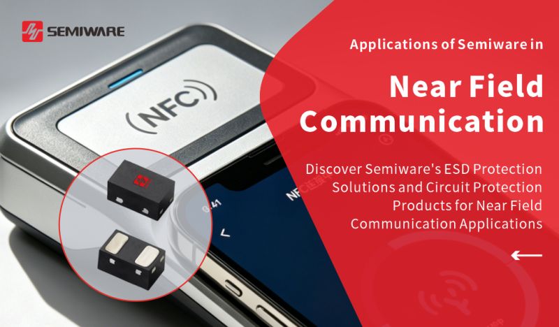
To address the requirements for small size, low parasitic capacitance, and high ESD reliability in portable devices like mobile phones and wearables, Semiware has introduced a range of ESD protection devices. Among them, the SE06F10B18UA is specifically designed for NFC and various RF antenna applications.
The device utilizes a DFN0603 package, measuring just 0.6 mm × 0.3 mm × 0.3 mm; its ultra-compact size makes it ideal for integration into compact NFC modules and high-density PCB layouts within mobile phones.
Conclusion
Although NFC antennas facilitate wireless communication, they remain vulnerable to ESD strikes from human contact and the external environment. For portable devices like mobile phones, appropriate ESD protection can mitigate the impact of static electricity on the NFC controller and communication functionality.
If you are designing ESD protection for NFC antennas, RF antennas, or mobile devices, the Semiware technical team can provide component selection support tailored to your specific circuit and application requirements.
To learn more about ESD protection solutions for NFC interfaces, please visit the Semiware NFC reference design.
Or contact us for product and selection support.