Introduction
PROFIBUS is widely used in factory production lines, process industries, and PLC distributed I/O systems. Engineers frequently encounter a common field issue: equipment passes laboratory testing successfully, yet during actual operation on the factory floor, nodes randomly drop offline or communication experiences intermittent interruptions. Upon inspection, the transceiver chips appear intact with no visible signs of burnout. Such failures are highly likely caused by latent damage resulting from Electrostatic Discharge (ESD).
Drawing on Semiware's circuit reference designs, this article outlines a practical interface protection strategy, covering the fundamental characteristics of PROFIBUS-DP, ESD risks, key protection considerations, and component selection.
I. Core Characteristics of PROFIBUS
PROFIBUS is an open industrial fieldbus managed by the PI organization. Its standards are based on IEC 61158 Type 3 / EN 50170. The mainstream variant is PROFIBUS-DP, which is specifically designed for distributed peripheral communication. Its key characteristics include:
- RS-485 Differential Transmission
The physical layer of PROFIBUS-DP utilizes RS-485 differential signaling, transmitting data via two signal lines (A and B).
- Multi-node Bus Structure
PROFIBUS-DP supports the connection of multiple devices—such as PLCs, remote I/O units, drives, and other field devices—to a single bus.
- Designed for Industrial Field Applications
PROFIBUS-DP is extensively used in factory automation, production lines, and process control. Equipment must typically withstand electromagnetic and transient interference generated by various industrial devices.
- Bus Topology
It employs a multi-point bus topology where a single cable connects multiple field devices in a daisy-chain configuration; devices often require on-site hot-swapping and commissioning.
II. Why PROFIBUS Requires ESD Protection Design
2.1 Limited on-chip ESD capability of transceivers: The energy from contact or air discharges in industrial environments can easily exceed the limits of the chip's built-in protection.
2.2 Multiple sources of static electricity in the field: Static discharge events can be triggered by actions such as hot-swapping PROFIBUS communication connectors, personnel touching connectors, equipment installation and maintenance, cable friction, and potential differences between devices.
2.3 Faults are often insidious: ESD strikes do not necessarily cause immediate chip breakdown; in some cases, they may result in device performance degradation or latent damage.
2.4 Impact of single-node failure on the bus in multi-node architectures: If the RS-485 physical layer of a specific node is damaged or malfunctions, it can—under certain conditions—compromise the communication stability of the entire bus.
III. Key Considerations for PROFIBUS-DP ESD Protection
3.1 Protection Targets: A/B Differential Bus Lines
The A and B differential lines connect directly to external communication cables, serving as the primary entry points for static electricity onto the PCB.
Therefore, ESD protection">ESD protection components should generally be placed on the A/B signal lines. Discharge paths for connector metal housings and shielding layers must be designed in conjunction with the system's overall grounding structure.
3.2 Low Junction Capacitance
PROFIBUS-DP supports communication speeds up to 12 Mbit/s; therefore, low-capacitance TVS (Transient Voltage Suppressor) devices are recommended.
3.3 Protection Architecture: TVS Clamping Combined with Current-Limiting Resistors
TVS devices are connected in parallel between the A/B lines and GND to clamp high ESD voltages to safe levels. Small-value current-limiting resistors connected in series help dissipate surge current and protect the transceiver; however, the resistance value must be kept low to avoid affecting the differential signal amplitude.
3.4 Critical Aspects of PCB Layout
ESD components must be placed as close as possible to the connector pins to minimize the trace length between the TVS and the connector, thereby reducing loop inductance.
The protection ground must be connected to the connector's shielding shell (PE/protective ground) via the shortest possible path; routing it to the mainboard's digital ground—which involves a longer path—would result in high impedance for the electrostatic discharge path, rendering the protection ineffective.
IV. Semiware PROFIBUS-DP ESD Protection Device Selection Guide
This solution is designed for PROFIBUS-DP bus ports, meeting IEC 61000-4-2 system-level ESD testing standards while supporting data rates from 9.6 kbps to 12 Mbps.
Semiware Recommended Devices:
- SESRV05-4A — 5 V ESD protection">ESD protection diode, with 0.4 pF typical capacitance and ±15 kV ESD protection">ESD protection.
- SRV05-4 — 5 V ESD protection">ESD protection diode, featuring 0.6 pF typical capacitance and ±15 kV ESD protection">ESD protection.
Reference Design Block Diagram:
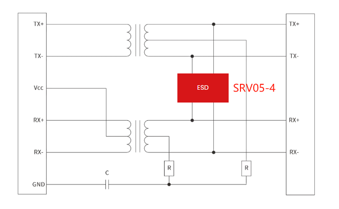
To learn more, please visit: https://en.semiware.com/reference-designs/profibus/
Summary
In industrial environments, activities such as hot-swapping, human contact, equipment maintenance, and other transient events can pose ESD risks.
If your PROFIBUS-DP product is undergoing ESD testing or experiencing issues like communication dropouts in the field, in addition to checking communication protocols, termination matching, and cabling, you should also evaluate the interface design regarding ESD components, parasitic capacitance, PCB layout, and the integrity of the discharge path.