Introduction
TVS (Transient Voltage Suppressor) diodes are widely used in circuits—such as power ports, signal interfaces, communication lines, industrial equipment, and automotive electronics—to suppress transient overvoltages like ESD and surges, thereby mitigating the impact of overvoltage on sensitive downstream components.
However, during product development, reliability testing, and mass production, engineers frequently encounter a recurring issue: TVS diodes repeatedly fail, burn out, or short-circuit—with faults persisting even after the component is replaced.
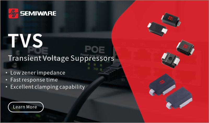
This article analyzes the issue from three perspectives—common failure symptoms, root causes, and engineering solutions—and offers practical advice to electronics engineers regarding TVS selection and EMC protection design.
I. Typical Symptoms of TVS Failure
Failed TVS diodes exhibit distinct and persistent abnormal behavior during circuit operation. Typical failure modes include:
- Short-circuit burnout: The TVS diode enters a permanent short-circuit state, causing power loss, interface failure, or a drop in board-level power performance.
- Performance degradation: The TVS does not burn out completely but loses its transient suppression capability, leading to failures in ESD/surge tests and unstable circuit protection.
- Intermittent failure: The TVS functions correctly under normal conditions but fails during high-temperature operation, surge events, or prolonged use, resulting in intermittent product malfunctions.
- Cracking and aging: Prolonged operation at excessive temperatures can cause package cracking, parameter drift, and premature failure due to aging.
II. Causes of Repeated TVS Failure
Most instances of TVS burnout are not caused by component quality issues but rather by flawed circuit design, mismatched parameters, or improper layout.
2.1 Continuous Overvoltage
TVS diodes are designed to suppress transient surges, not to withstand continuous overvoltage. If the circuit's operating voltage consistently exceeds the TVS's maximum working voltage, the component is subjected to a sustained power load; this leads to heat accumulation and, ultimately, permanent burnout. This issue is frequently encountered in power interface protection circuits.
2.2 Transient Energy Overload
Events such as electrostatic discharge (ESD), lightning surges, hot-plugging transients, and industrial electromagnetic pulses can deliver extremely high levels of transient energy. If the TVS's rated power and clamping voltage do not match the circuit's actual surge energy, the instantaneous energy will exceed the component's tolerance limits, resulting in breakdown damage.
2.3 Improper TVS Parameter Selection
Blindly selecting general-purpose TVS models is a major design error. Common mismatches include insufficient power ratings, unsuitable breakdown voltages, and signal-line TVS capacitance that does not meet high-speed signal requirements. Undersized parameters result in inadequate protection, while oversized parameters lead to unnecessary cost and signal distortion.
2.4 Over-temperature and Poor Heat Dissipation
Excessive ambient temperatures, localized heat accumulation on the PCB, or frequent, prolonged surge events can cause the TVS junction temperature to exceed its limits. Poor PCB thermal design exacerbates heat buildup, leading to thermal runaway and component failure.
2.5 Improper PCB Layout Design
Substandard EMC layout practices pose a risk of repeated TVS damage. Excessively long surge current paths, improper grounding, and inadequate series resistance matching prevent the effective dissipation of surge energy, thereby stressing the TVS and accelerating its failure.
2.6 Poor Component Quality and Batch Inconsistency
Low-quality TVS products often suffer from defects in wafer materials, packaging processes, and parameter consistency. Such components fail to withstand standard surge tests and are prone to batch-related failures during mass production.
III. How to Prevent TVS Diode Failure
Resolving the issue of recurring TVS failure requires optimization across several areas, including component selection, circuit design, PCB layout, and thermal design.
3.1 Selecting the Right TVS Based on Actual Operating Conditions
TVS selection should be based on an assessment of the circuit's actual operating conditions and the transient environment.
- For power interfaces, the focus should be on the TVS's surge current and pulse power handling capabilities.
- For high-speed signal interfaces, priority should be given to low capacitance and signal integrity.
3.2 Optimizing EMC PCB Layout
A robust PCB layout ensures that transient currents have a low-impedance, short-path discharge route while preventing surge currents from entering sensitive circuits.
The following principles are recommended:
- Place TVS devices as close as possible to external interfaces.
- Minimize the surge current loop area.
- Shorten TVS trace lengths.
- Reduce parasitic inductance.
- Optimize grounding and return paths.
- Avoid placing sensitive components within the surge current path.
For complex applications, a coordinated protection network can be constructed using components such as resistors, inductors, capacitors, and common-mode chokes, tailored to specific requirements.
3.3 Optimizing Thermal Design
For high-power applications or those subject to repetitive surges, thermal design should be integrated into the TVS protection scheme to ensure the TVS operates within specified electrical and thermal stress limits under actual working conditions.
Heat dissipation can be improved by:
- Increasing the effective copper area on the PCB.
- Optimizing heat conduction paths.
- Properly spacing components.
- Keeping TVS devices away from high-temperature heat sources.
3.4 Implementing Multi-Stage Protection
For complex or high-risk applications, a single TVS device may not suffice to meet comprehensive protection requirements. A multi-stage protection scheme can be created by coordinating the TVS with other protective components such as fuses, varistors (MOVs), gas discharge tubes (GDTs), inductors, and filtering devices.
IV. Semiware TVS and EMC Circuit Protection Solutions
Semiware Semiconductor specializes in TVS, ESD, and other circuit protection devices, offering EMC protection design support for power and signal interfaces.
Semiware offers:
- A wide range of TVS products: Covering various operating voltages, power ratings, and package types to meet the protection needs of different power and signal interfaces.
- Power and signal protection solutions: Providing circuit protection support for applications such as industrial equipment, consumer electronics, automotive electronics, and communication equipment.
- EMC pre-testing and solution optimization: Identifying potential ESD and surge protection issues through early-stage testing.
- Technical support from engineers: Assisting customers with TVS selection, circuit design, and PCB protection layout.
- Prevention of over-design: Striking a balance between protection performance, reliability, signal integrity, and cost.
By integrating component selection, circuit design, PCB layout, and EMC testing, it is possible to reduce the risk of recurrent TVS failures, enhance product reliability, and minimize the time and costs associated with repeated validation.
If you are experiencing issues such as repeated TVS failures, failure to pass ESD or surge tests, or difficulties in selecting the right TVS, please contact the Semiware engineering team to obtain circuit protection solutions tailored to your specific applications.