I. Introduction: Why Does a Correctly Selected TVS Still Fail?
In the design of high-speed interfaces and complex electronic systems, a frequently perplexing question arises:
Even when a TVS device meeting the IEC 61000-4-2 Level 4 standard—and even nominally rated for ±30kV ESD immunity—has been selected, why do products still experience ESD breakdown or system anomalies during the mass production phase?
Engineers typically focus on the static parameters listed in datasheets while overlooking the device's actual performance under nanosecond-scale transient surges—specifically, its dynamic clamping capability (or TLP behavior) under transient conditions.
II. The Nature of ESD: Nanosecond-Scale, High-Energy Surges
ESD (Electrostatic Discharge) is not a gentle DC power source; rather, it is a highly destructive transient energy pulse. According to the IEC 61000-4-2 standard, an 8kV contact discharge is characterized by the following:
- Extremely Fast Rise Time: < 1 ns
- Extremely High Peak Current: The peak current can instantaneously reach over 30A.
This implies that a device's performance is determined by its dynamic resistance and transient clamping capability, rather than its static parameters.
III. Datasheet Pitfalls: Static Parameters ≠ Dynamic Protection Capability
When selecting components, engineers primarily focus on VRWM (Reverse Standoff Voltage) and VC (Clamping Voltage) values derived from 8/20µs waveform tests as presented in datasheets.
However, the rise time of an 8/20µs waveform is significantly slower than that of a genuine ESD surge.
The Reason:
- Under nanosecond-scale, high-current surges, a TVS device no longer behaves as an ideal switch;
- instead, its internal parasitic inductance and dynamic resistance become the dominant factors governing the effectiveness of its voltage clamping—a phenomenon characterized by its TLP response.
IV. TLP Curves: Essentially a Reflection of a TVS’s "Real-World Performance"
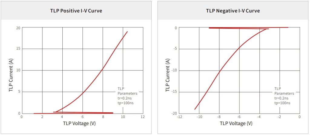
TLP curves simulate a realistic ESD environment. When interpreting these curves, we primarily focus on three key points:
1. Dynamic Resistance (RDYN): The steeper the slope of the curve after breakdown (i.e., the closer it is to vertical), the lower the dynamic resistance. This signifies that even if the current surges significantly, the voltage will not rise drastically in tandem.
2. The 16A Rule: Locate the 16A point on the TLP curve (which corresponds to the typical effective current of an 8kV contact discharge). The corresponding voltage value at this point represents the actual voltage that your chip is subjected to.
3. Snapback Characteristics: For high-performance TVS devices, the voltage drops rapidly to a lower level immediately after triggering. This characteristic is particularly crucial for the protection of high-speed interfaces.
V. Real-World Comparison: Semiware vs. International Brands
In the context of USB 3.0 interface protection solutions, we compared the key parameters of Semiware’s SE10F04B3.6UA-SP TVS Diode Array against Infineon’s ESD113-B1-02EL.
| Parameter | ESD113-B1-02EL (Infineon) | SE10F04B3.6UA-SP (Semiware) |
| VRWM | 3.3V | 3.6V |
| VBR | 4V | 4V |
| Package | DFN1006-2 | DFN1006-2 |
| IPP | 6A | 3A |
| VC @1A | 3.8V | 6V |
| VC @3A | 4.5V | 8V |
| VC @6A | 5.5V | 20V |
| VC @TLP 16A | 9.4V | 14V |
| RDYN | 0.3 Ω | 0.45 Ω |
| CJ | 0.22 pF | 0.2 pF |
| ESD Air | ±20 kV | ±20 kV |
Although the static ESD withstand ratings for both devices are comparable, during the TLP 16A test—which simulates a real-world ESD transient:
Semiware SE10F04B3.6UA-SP exhibited a clamping voltage of 9.4V;
Infineon ESD113-B1-02EL measured 14V.
Clearly, the SE10F04B3.6UA-SP offers a significantly larger safety margin.
VI. PCB Layout: How to Select Components Like an Expert?
- Layout: Minimize "Dynamic Inductance"
No matter how fast a TVS responds, it cannot outpace the parasitic inductance generated by the PCB traces themselves.
Rule: The TVS must be placed in immediate proximity to the specific I/O port or power pin requiring protection.
Routing: Ensure that the via connecting the TVS to GND is as short and wide (low-impedance) as possible. The signal path should pass through the TVS before entering the downstream chip, utilizing a "forking" principle to divert the transient energy away.
- Component Selection: Focus on VC (Clamping Voltage) as Much as VRWM (Working Voltage)
Beyond static parameters, pay close attention to the clamping voltage waveforms (per IEC 61000-4-2) or the TLP curves provided in the datasheet. Ensure that the clamping voltage—at the maximum specified peak pulse current (IPP)—remains below the maximum rated voltage of the protected chip.
- High-Speed Signals Require Low Capacitance
For interfaces such as HDMI 2.1 (12Gbps) or USB 3.2 Gen 2 (10Gbps), it is imperative to select ultra-low capacitance ESD diodes (typically <0.5pF)—preferably those featuring "Snapback" characteristics—or to utilize integrated ESD suppressors that incorporate TVS technology. The Snapback-feature ESD devices developed by Semiware ensure signal integrity while delivering extremely low clamping voltages.
Conclusion
ESD protection is not a matter of mysticism; rather, it is a contest of nanosecond-scale response speeds and dynamic resistance.
As the comparison above demonstrates, Semiware’s performance regarding key dynamic parameters rivals that of international brands—and even holds a distinct advantage in terms of low clamping voltage and capacitance control.
👉 Explore Semiware’s ESD protection portfolio and TLP-verified TVS solutions to improve system-level robustness.


Comments (0)