Protection Devices-TVS Diodes-ESD Protection devices-Gas Discharge Tube-Thyristor-Pled Protectors-Mov Protection Devices-TVS Diodes-ESD Protection devices-Gas Discharge Tube-Thyristor-Pled Protectors-Mov
  • Product
  • Application
  • Reference
  • Quality & Resources
  • Support
    • Technical Support
    • Sample Request
    • EMC Rectification and Testing
  • About Us
  • Contact Us
首页 Technical EMC Design Guidelines for High-Speed PCB Layout: Four Fundamental Rules to Reduce EMI

EMC Design Guidelines for High-Speed PCB Layout: Four Fundamental Rules to Reduce EMI

Bella 2 days ago

In modern electronic systems, electromagnetic compatibility (EMC) issues are often not caused by component failures, but by improper PCB layout and current path design.

High-speed signals, especially in MHz to GHz range, are highly sensitive to layout structure. Small design mistakes can significantly increase electromagnetic interference (EMI), leading to failed compliance testing and unstable system performance.

This article summarizes four fundamental EMC design rules based on practical engineering experience.

EMC Design Guidelines for High-Speed PCB Layout: Four Fundamental Rules to Reduce EMI-Protection Devices-TVS Diodes-ESD Protection devices-Gas Discharge Tube-Thyristor-Pled Protectors-Mov
  1. Minimize Current Loop Area (Ensure a Short Return Path)

At high frequencies, current does not simply take the lowest resistance path—it follows the lowest inductance path.

This means signal current and return current must remain tightly coupled.

Key principles:

  • Signal trace and return path should be closely aligned
  • High-speed signals must have an adjacent reference ground plane
  • Larger loop area directly increases radiated emissions

Design recommendation:

Keep signal layer and ground plane as close as possible to minimize loop inductance and reduce EMI.

  1. Maintain a Continuous Reference Ground Plane

A stable and continuous ground plane is critical for maintaining predictable return current paths.

When the ground plane is split or interrupted:

  • Return current is forced to detour
  • Loop impedance increases
  • EMI emissions significantly rise

Important guideline:

In most high-speed designs, a continuous ground plane is preferred over segmented grounding structures.

Exception cases:

Only isolated low-frequency or sensitive analog sections may require separated return paths, and even then, careful planning is required.

  1. Avoid Routing High-Speed Signals Between Connectors

Connectors act as natural electromagnetic entry and exit points for noise.

When high-speed signals are placed between connectors:

  • Voltage differences between connectors increase
  • External cables can easily pick up noise
  • Radiated emissions are amplified
  • Layout best practice:
  • Place connectors on one side of the PCB whenever possible
  • Keep high-speed traces away from connector-to-connector regions
  • Avoid routing sensitive signals through “connector corridors”
  1. Control Signal Edge Rate (Do Not Chase the Fastest Transition)

Faster signal edges generate higher-frequency harmonics.

For example:

  • 1 ns edge → harmonic content up to GHz range
  • 5 ns edge → significantly reduced high-frequency EMI components

Design insight:

Faster is not always better. In many cases, slightly slowing down the transition time can greatly improve EMC performance without affecting functionality.

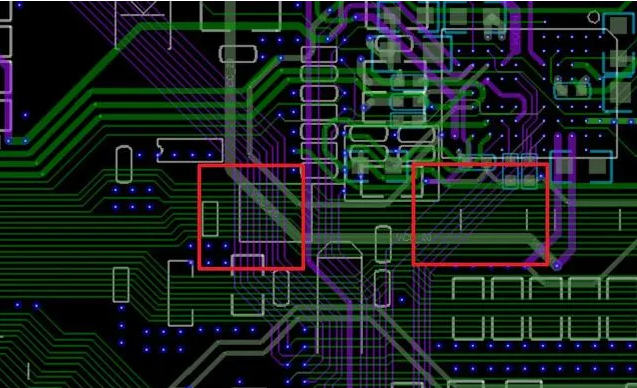
📌 Typical EMC Risk Example in PCB Layout

The image below illustrates a typical high-speed PCB layout where multiple EMC issues can occur:

  • Disrupted return paths
  • Cross-region high-speed routing
  • Connector-induced coupling effects
  • Increased loop area due to improper routing

👉 These layout patterns are common root causes of EMC test failures.

Conclusion

EMC design is not about adding more protection components. It is fundamentally about controlling how current flows on the PCB.

A well-designed high-speed system always ensures:

  • Controlled current paths
  • Continuous return planes
  • Proper signal routing architecture
  • Managed switching behavior

When these principles are followed, EMC performance becomes predictable and stable.

# EMC design# PCB Layout
0
Bella
Your Circuit Protection Solutions Provider

Comments (0)

Back
    Leave a comment

Related Posts

  • Analysis of Electrostatic Discharge (ESD) and Surge Protection Schemes for Power Conversion Systems (PCS)
  • 48V DC SELV Power Supply Surge, ESD, and Overcurrent Comprehensive Protection Solution
  • IP Camera Interface Protection: RJ45, USB, SD Card and Power Design Guide
  • Low-Capacitance, Dual-Channel ESD Protection Solution for High-Speed ​​Signals
  • SPM3401S as an Alternative to AO3401: A Pin-to-Pin Compatible P-Channel MOSFET Solution

Search

About Semiware

https://en.semiware.com/blog/wp-content/uploads/2023/09/start.mp4

Latest News

Robotic Vacuum Cleaner ESD Protection Guide: TVS, GDT & Surge Design Solutions
2 months ago
RS485 vs CAN Bus: Key Differences and Surge & ESD Protection Solutions | Semiware
3 months ago
How to Protect 48V Automotive Power and CAN Bus from ESD and Surge
3 months ago

Tags

1.5KE series (65) 1500W TVS Diode (49) 5000W TVS diode (26) Automotive TVS Diode (67) bulk supplier tvs diode (48) BZT52 datasheet (30) BZT52C Zener diode (27) do-214aa sidactor (37) do214ab (49) do214ab diode (49) do 214ab tvs diode (49) do214ab vs smc (49) Low voltage TVS Diode (27) p4ke tvs diode (33) p4sma protection diode (59) p4sma transient suppressor (61) ptc fuse smd (38) smaj diodes (88) SMAJ diode specifications (31) SMAJ diode supplier (33) sma tvs diode (90) smbj diode (77) SMB package TVS (32) SMB sidactor overvoltage protection (33) SMC diode (49) smc do 214ab (49) smcj (49) smcj diode (49) smcj tvs diode (49) SMC tvs diode (52) smd tvs diode (94) SOD 123FL TVS diode (83) surface mount ptc fuse (38) surface mount TVS diode (34) Transient Voltage Suppression Diode 1500W (51) tvs diode 1.5kw (44) TVS diode application (35) tvs diode distributor (43) TVS diode for circuit protection (49) tvs diode manufacturer (31) tvs diode manufacturers (98) TVS diode parameters (90) TVS diode price (34) tvs diode smcj (49) vishay tvs diode equivalent (28)
Hey, I am Cassie, any inquiry, welcome to contact
  • +86-15216658399
  • Product
  • Application
  • Reference
  • Quality & Resources
  • Support
  • About Us
  • Contact Us
Copyright © 2026 Protection Devices-TVS Diodes-ESD Protection devices-Gas Discharge Tube-Thyristor-Pled Protectors-Mov. Designed by Semiware Oversea Team.
Partners: Semiware EMC Test TVS Diodes ESD Diodes Polymers Protection Thyristors PLED Gas Discharge Tubes ZnO Varistors Mosfets Diodes PTC SCR&Triacs
  • Product
  • Application
  • Reference
  • Quality & Resources
  • Support
    • Technical Support
    • Sample Request
    • EMC Rectification and Testing
  • About Us
  • Contact Us