I. Overview
The SI2302 is one of the most common N-channel MOSFET models in the SOT-23 package, widely used in consumer electronics, power management, and compact control circuits. To address the needs of low-voltage load switching, battery-powered equipment, and space-constrained electronic products, Semiware has introduced the SNM2302. This is a 20V enhancement-mode N-channel MOSFET housed in a compact SOT-23 package.
The SNM2302 combines low on-resistance, low gate charge, and logic-level drive capabilities. With a product profile similar to the SI2302, it serves as a viable alternative or secondary source option, making it suitable for new product development, BOM optimization, and supply chain diversification initiatives.
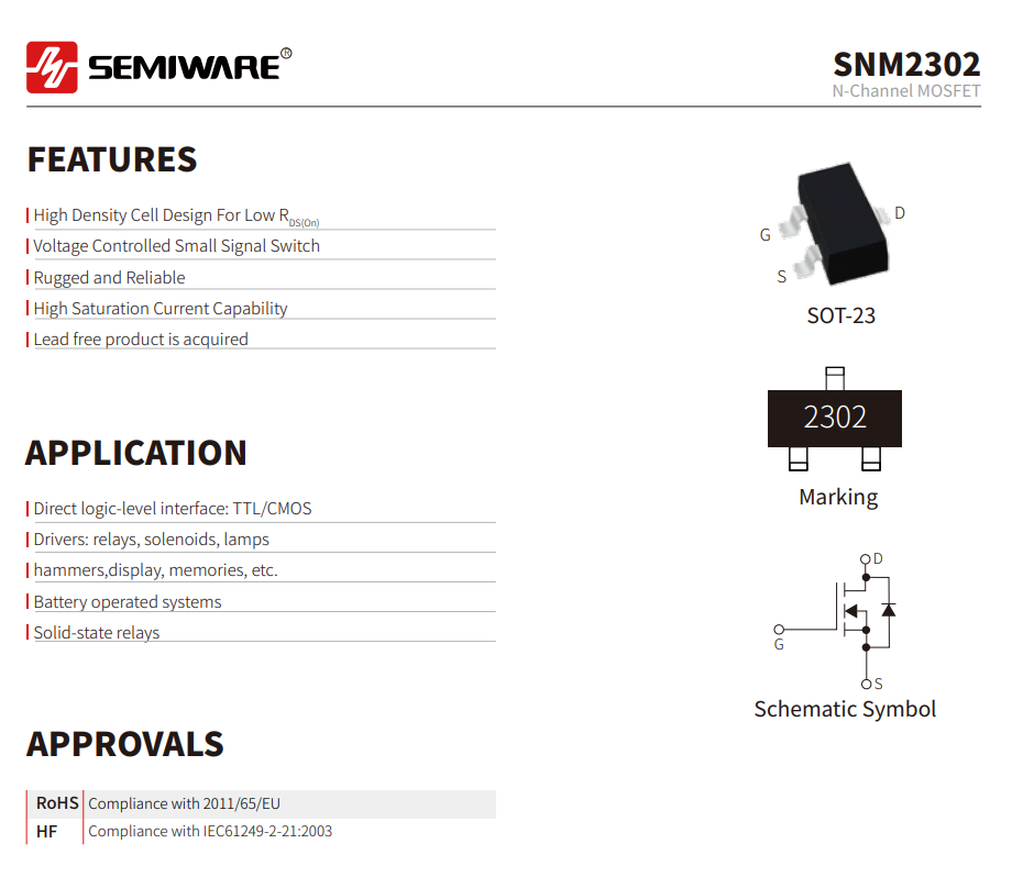
II. SNM2302 Mosfet Key Electrical Parameters
| Parameter | Specification |
| Drain-Source Voltage (V<sub>DSS</sub>) | 20 V |
| Continuous Drain Current (I<sub>D</sub>) | 2.3 A @ T<sub>A</sub> = 25°C |
| Gate-Source Voltage (V<sub>GS</sub>) | ±12 V |
| R<sub>DS(on)</sub> | 55 mΩ typ., 85 mΩ max. @ V<sub>GS</sub> = 4.5 V |
| R<sub>DS(on)</sub> | 70 mΩ typ., 125 mΩ max. @ V<sub>GS</sub> = 2.5 V |
| Gate-Source Threshold Voltage (VGS(th)) | 0.7 V typ. |
| Total Gate Charge (Q<sub>g</sub>) | 4.0 nC typ., 10 nC max. |
| Package | SOT-23 |
III. Key Features of the SNM2302 MOSFET
- Compact SOT-23 Package: Ideal for consumer electronics, portable devices, and small control modules where PCB space is limited; offers package and pin compatibility for many SI2302 applications.
- Low RDS(on): Low on-resistance helps minimize conduction losses and device heat generation.
- Logic-Level Drive: Specified RDS(on) performance at low gate drive voltages, making it suitable for switching applications controlled by MCUs and other low-voltage logic circuits.
- Low Gate Charge: Typical total gate charge of 5.5nC helps reduce gate drive losses and supports PWM switching control across a range of frequencies.
- Good Current-Carrying Capability: Continuous drain current up to 2.3A, suitable for small load switches and low-voltage drive circuits; actual operating current should be derated based on package thermal conditions.
- RoHS Compliant: Meets lead-free and environmental standards, satisfying regulatory requirements for consumer and industrial electronics.
IV. Typical Application Scenarios
- Load Switch Circuits
The SNM2302 can be used in MCU-controlled low-voltage load switches to manage power (switching on/off) for sensors, LEDs, small peripherals, and other peripheral modules.
Typical applications include:
- Sensor power switching
- LED load switching
- USB and peripheral device power control
- Display module power control
- Small peripheral power management
- Battery-Powered Devices
- In portable instruments, handheld devices, and other battery-powered products, MOSFETs are commonly used for power path switching and load management.
- MCU-Controlled Low-Voltage Switching
- The SNM2302 supports logic-level driving and can be controlled by 3.3V or 5V logic signals, making it suitable for switching control between an MCU and low-voltage loads.
- Small Driver Units
- The SNM2302 can serve as a low-side switching device to drive loads such as relays, solenoid valves, and low-power indicator lights.
- Consumer Electronics and IoT Devices
With its compact SOT-23 package, low on-resistance, and logic-level drive capability, the SNM2302 is suitable for:
- Consumer electronic devices
- Smart home and IoT terminal devices
- Small home appliance control boards
- Industrial control boards
- Portable electronic devices
- Auxiliary power control for display and storage modules
V. Design Considerations and Recommendations
- Derating
- The SNM2302 has a rated VDSS of 20V. In actual circuit designs, a reasonable voltage margin should be maintained—accounting for system operating voltage, transient spikes, and load fluctuations—rather than operating simply at the maximum rated limit.
- Gate Driving
- The SNM2302 supports logic-level driving, with a maximum VGS rating of ±8V. Designs must ensure the gate-source voltage does not exceed this rated range.
- For 3.3V or other low-voltage drive systems, it is crucial to verify that the RDS(on) meets requirements at the target operating current.
- PCB Layout
- For PWM and other high-speed switching applications, trace lengths for the gate drive loop and power loop should be minimized to reduce parasitic inductance, thereby mitigating voltage ringing and switching noise.
4. Thermal Design
- The actual temperature rise of the MOSFET depends not only on RDS(on) but also on operating current, switching frequency, gate drive conditions, PCB copper area, and ambient temperature.
- Therefore, in high-load or high-frequency applications, actual testing should be conducted to verify that the device junction temperature remains within permissible limits.
- Supply Chain and BOM Optimization
- For projects utilizing the SI2302 or similar low-voltage MOSFETs, the SNM2302 can be evaluated as a second-source or alternative component. This helps expand sourcing options and optimizes the Bill of Materials (BOM) regarding device cost, lead times, and volume supply.
Summary
If you are evaluating alternatives to the SI2302 or similar low-voltage MOSFETs, please contact Semiware. By providing details such as the target part number, operating voltage, load current, and gate drive conditions, you can receive assistance with part evaluation and sample verification.