Overview
In power conversion equipment such as high-frequency switching power supplies, UPS systems, and electronic ballasts, 650V high-voltage MOSFETs must strike a balance between voltage withstand capability, conduction losses, and switching performance. For designs utilizing 20N65F MOSFET, engineers and procurement teams prioritize not only electrical parameters but also package compatibility, supply availability, and overall BOM costs.
The Semiware SNM20N65F is a 650V N-Channel MOSFET housed in an insulated TO-220F package, serving as a viable alternative to existing 20N65F Mosfet.
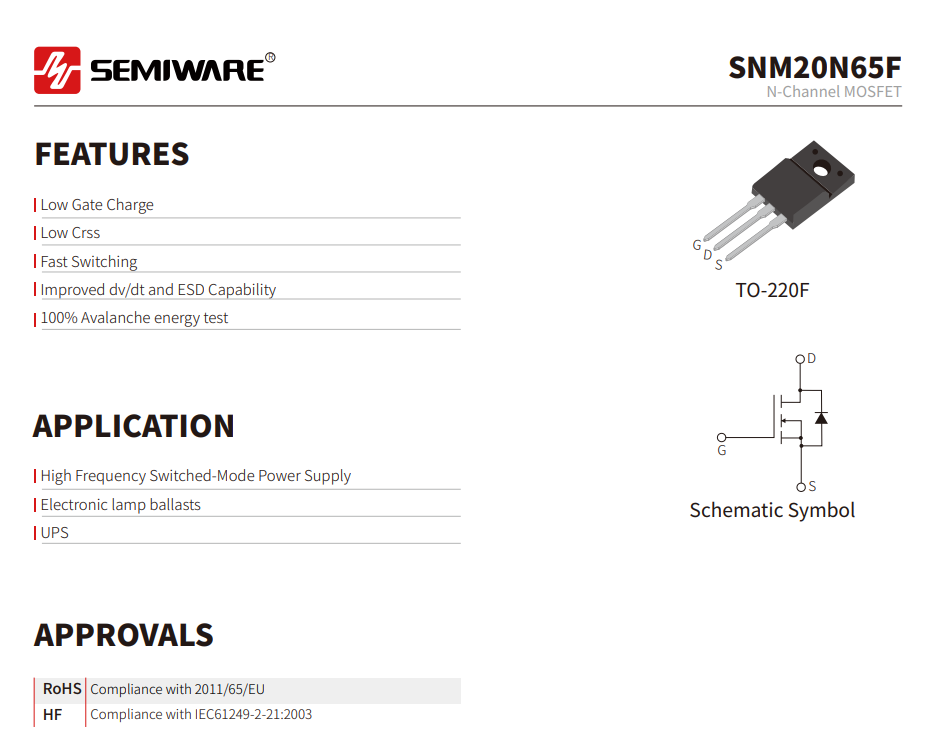
I. Key Electrical Parameters of the SNM20N65F MOSFET
| Parameter | SNM20N65F |
| Drain-Source Voltage | 650V |
| Continuous Drain Current | 20 A |
| Pulsed Drain Current | 80A |
| Gate-Source Voltage | ±30 V |
| Drain-Source On-Resistance | 0.36 Ω |
| Total Gate Charge | 59 nC |
| Single-Pulse Avalanche Energy | 720 mJ |
| Power Dissipation | 50 W |
II. SNM20N65F MOSFET Key Features
2.1 High Voltage and Current Ratings
- With a 650V rating and 20A continuous drain current, the SNM20N65F is suitable for off-line power conversion scenarios requiring substantial voltage headroom and current-handling capability.
2.2 Low On-Resistance
- The SNM20N65F features a typical RDS(on) of 0.36Ω. Low on-resistance minimizes conduction losses; for applications such as high-power switching power supplies and UPS systems, this enables designers to achieve a superior balance between conduction loss and thermal management.
2.3 Low Gate Charge
- In high-frequency PWM switching circuits, gate charge and parasitic capacitance influence MOSFET drive losses and switching dynamics.
2.4 100% Avalanche Energy Test
- This parameter evaluates the MOSFET's ability to withstand transient energy under specific single-pulse avalanche conditions, providing design margin against transient stresses caused by transformer leakage inductance, parasitic parameters, and switching operations.
III. SNM20N65F MOSFET Application Scenarios
3.1 High-Frequency Switched-Mode Power Supply (SMPS)
- High-frequency SMPS applications impose comprehensive requirements on MOSFETs regarding voltage withstand, conduction losses, and switching performance. The SNM20N65F’s 650V voltage rating, low RDS(on), and low Crss characteristics make it suitable for use as a power switch in high-frequency, off-line switching power supplies.
3.2 Electronic Lamp Ballasts
- Electronic ballasts require MOSFETs to operate at high switching frequencies, necessitating consideration of conduction losses, switching losses, and thermal management. The SNM20N65F is suitable for designs involving high-voltage power switching stages in these applications.
3.3 UPS
- In UPS power conversion stages, MOSFETs must withstand high voltage and current stresses while balancing efficiency and thermal design requirements. The 20A-rated SNM20N65F is a viable option for component selection or as a replacement candidate in such power stages.
IV. MOSFET Replacement Verification
When replacing a 20N65F with the SNM20N65F, the following verification sequence is recommended:
- Pin-to-pin and package compatibility
- Static parameter comparison
- Gate-drive compatibility
- Switching waveform verification
- Temperature-rise testing
- Full-load and abnormal-condition testing
- Long-term reliability validation
Summary
For 650V high-voltage MOSFET applications, component replacement requires evaluating not only voltage and current ratings but also conduction losses, switching characteristics, thermal performance, and package compatibility.
If you are facing challenges regarding MOSFET cost control, lead times, or supply stability, please contact Semiware for component selection support. Our FAE team can assist with device selection and replacement verification based on your specific requirements for operating voltage, current, switching frequency, and packaging.