The Semiware SE16P6F10U5.0MB / SR05 / SRV05-4 / ULC0524P series are low-capacitance, multi-channel ESD protection arrays specifically designed for high-speed data interfaces.
This series effectively protects sensitive electronic equipment on communication lines from electrostatic discharge (ESD) and transient voltage surges, while also supporting high-speed signal transmission. It is one of the core solutions for high-speed interface protection.
I. Core Features and Advantages
| Model | Channels | Typical Applications | Electrical Characteristics |
| SE16P6F10U5.0MB | 2-channel | Gigabit Ethernet, USB 3.0, HDMI | Max junction capacitance Cj = 0.3pF |
| SR05 | 3-channel | USB 2.0 (2 I/O + Vbus) | Typical Cj = 2pF |
| SRV05-4 / ULC0524P | 4-channel | Fast Ethernet/Gigabit Ethernet, LVDS, SIM card interface, video interfaces | Typical Cj = 0.6pF, Max leakage current = 1nA |
Core Advantages:
- High Protection Capacity: Compliant with IEC 61000-4-2 / GB/T 17626.2 standards, it can withstand ±15kV air discharge and ±8kV contact discharge, achieving Level 4 protection.
- High-Speed Signal Compatibility: Ultra-low junction capacitance and low leakage current ensure distortion-free transmission of high-speed data interfaces.
- Multi-Channel Design: One device can protect multiple I/O channels, saving PCB area and simplifying layout.
II. Typical Application Areas
High-speed data interfaces: USB 2.0 / 3.0, USB OTG, FireWire, Ethernet
Video equipment: SVGA, HDMI, digital/analog video terminals
Mobile and communication devices: Mobile phones, tablets, portable electronic products
Other sensitive electronic devices: Scenarios requiring high-speed I/O ESD protection
III. Working Principle and Protection Mechanism
- Structure
Each channel consists of a pair of diodes. ESD current pulses are guided to GND through the diodes, achieving transient voltage clamping.
Typical Clamping Voltages:
- Human Model ESD: ±25V
- Contact Discharge: ±30V
- Air Discharge: ±30V
- Clamping Voltage Calculation
Ideal Circuit:
- Forward Pulse: VC = VCC + VF
- Reverse Pulse: VC = -VF
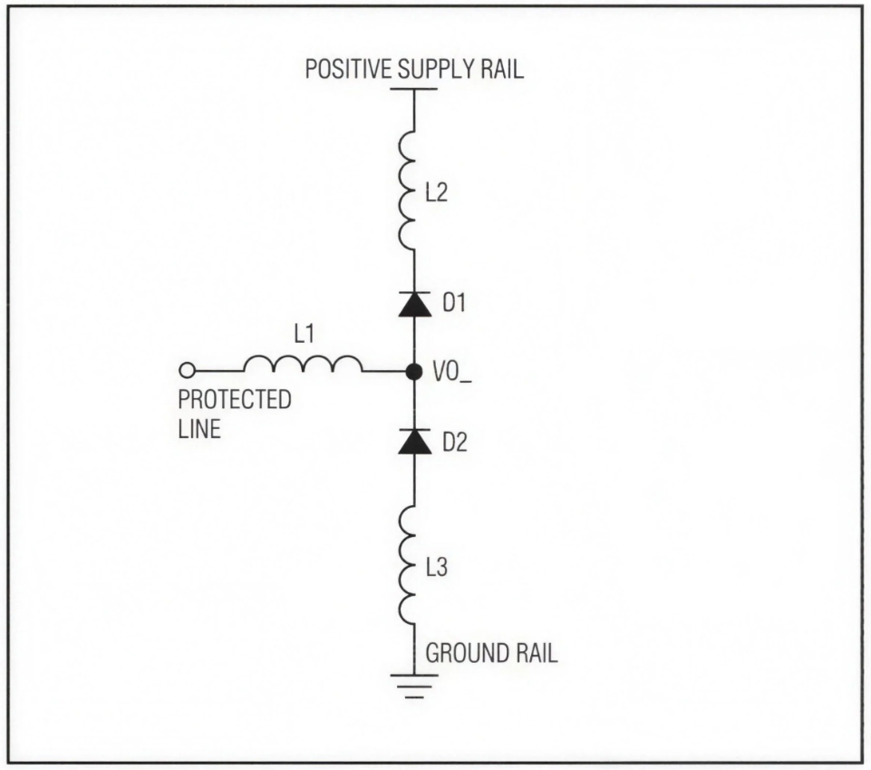
Actual PCB Routing Influence (Considering Parasitic Inductance L1/L2/L3):
👉 IESD is the ESD pulse current. Parasitic inductance significantly increases the actual clamping voltage; therefore, PCB routing optimization is crucial.
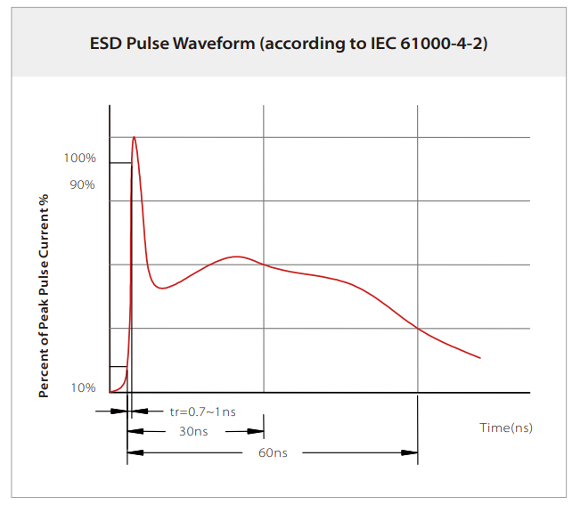
- ESD Current Characteristics
In an electrostatic discharge (ESD) event, the current pulse rises from 0 to its peak value within nanoseconds (see the figure above). For example:
An IEC 61000-4-2 ±15kV air discharge pulse can cause the current to rise to approximately 45A within 1ns (di/dt ≈ 45 × 10⁹ A/s). A mere 10nH inductor (approximately 12.7mm PCB trace) can add approximately 450V of clamping voltage.
Therefore, regardless of the nominal diode clamping voltage of the device, parasitic inductance caused by improper wiring will significantly increase the actual clamping voltage on the protected signal line.
- Bypass Capacitor Requirements
A 0.1μF low ESR ceramic capacitor connected in parallel between VCC and GND can absorb the charge from a ±8kV contact discharge.
Example of effective output impedance for the power rail: If it is 1Ω, the 24A spike current generated by a +8kV ESD pulse will add an additional VC ≈ 24V.
It is recommended to place bypass capacitors as close as possible to the VCC pin, and also to configure low ESR capacitors at the power supply terminals of the protected devices.
IV. Application Design PCB Layout Recommendations、
- Shorten the trace length from I/O interfaces to the ESD array;
- Use independent power and ground planes to reduce parasitic inductance;
- Ensure the return path of ESD transient current is as short as possible;
- Minimize conductive power and ground loops;
- Keep critical signals away from PCB edges to avoid coupling interference;
- Connect a low ESR ceramic capacitor in parallel between VCC and GND, as close as possible to the device pins;
- Connect a low ESR ceramic capacitor in parallel between the power supply terminal and GND of the protected device;
- Prioritize placing the ESD array near the I/O interface to ensure the shortest current return path and improve protection effectiveness;
- Multi-layer PCBs should ensure ground plane continuity to reduce local loop impedance.
If you are designing high-speed data interfaces or looking to improve system-level ESD robustness, our engineering team can help you:
- Select the optimal ESD array for your application
- Evaluate signal integrity vs. protection trade-offs
- Optimize PCB layout for better ESD performance
- Replace equivalent solutions from other suppliers
👉 Contact us today to discuss your design requirements and get application support from our FAE team.


Comments (0)